Method of reducing leakage current in sub one volt SOI circuits

a leakage current and soi circuit technology, applied in the field of integrated circuit power consumption reduction, can solve the problems of increasing chip power consumption, increasing cooling and packaging costs, and complex typical fets, and achieves reducing subthreshold leakage, reducing leakage, and reducing the effect of thresholds

Active Publication Date: 2005-02-24
GLOBALFOUNDRIES US INC
View PDF4 Cites 25 Cited by
  • Summary
  • Abstract
  • Description
  • Claims
  • Application Information

AI Technical Summary

Benefits of technology

The present invention relates to a multi-threshold integrated circuit (IC) with reduced subthreshold leakage and method of reducing leakage. Selectable supply switching devices (NFETs and/or PFETs) between a logic circuit and supply connections (Vdd and Ground) for the circuit have higher thresholds than normal circuit devices. Some devices may have the magnitude of threshol...

Problems solved by technology

Thus, not withstanding the decrease of chip supply voltage, chip power consumption has increased as well.
Both at the chip and system levels, cooling and packaging costs have escalated as a natural result of this increase in chip power.
So, ideal CMOS circuits use no static or DC power and only consume transient power from charging and discharging capacitive loads.
In practice however, typical FETs are much more complex than switches and transient power for circuit loads accounts for only a portion of CMOS circuit power consumption.
This is espec...

Method used


Image

  • Method of reducing leakage current in sub one volt SOI circuits
  • Method of reducing leakage current in sub one volt SOI circuits
  • Method of reducing leakage current in sub one volt SOI circuits

Examples


Embodiment Construction

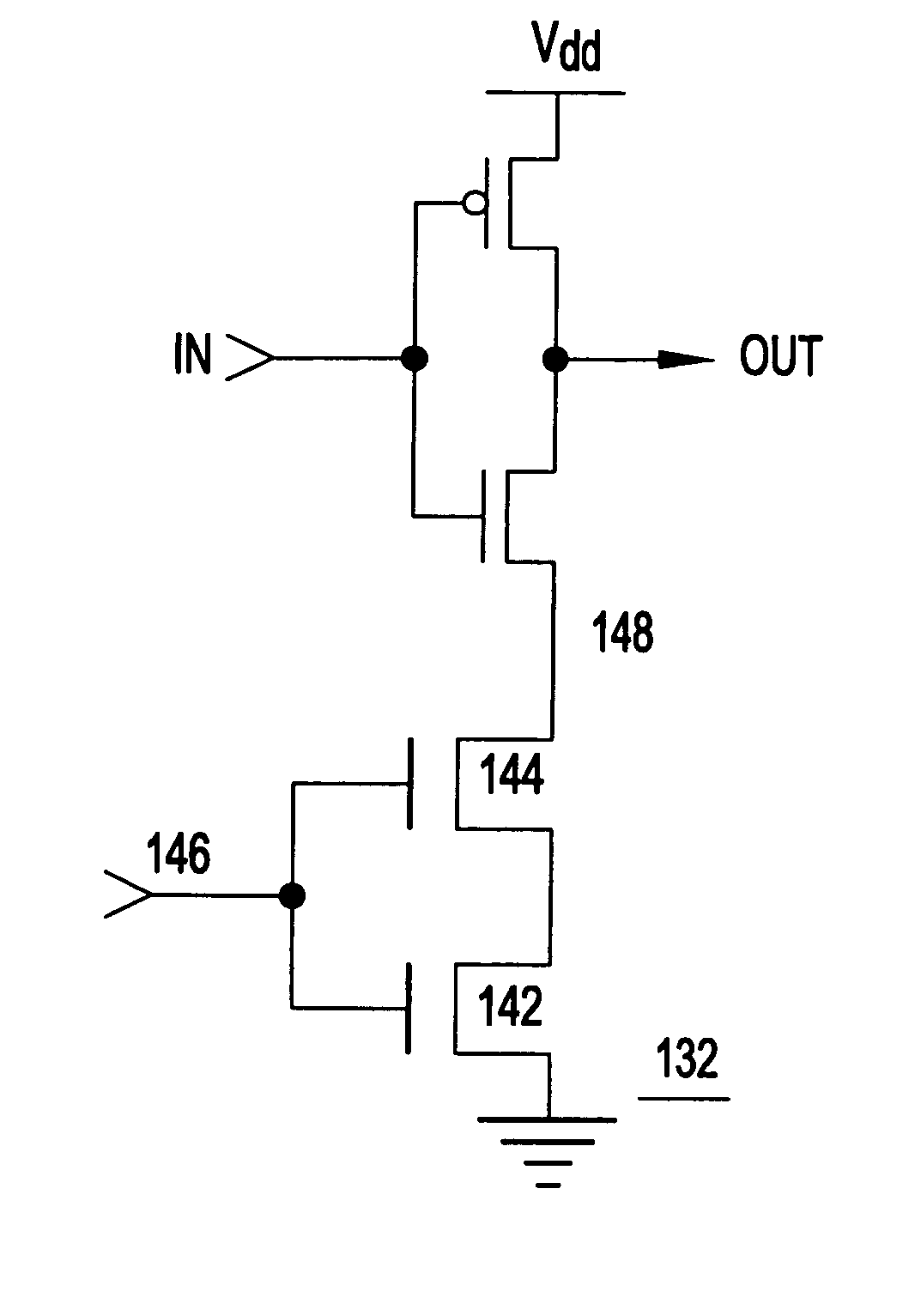
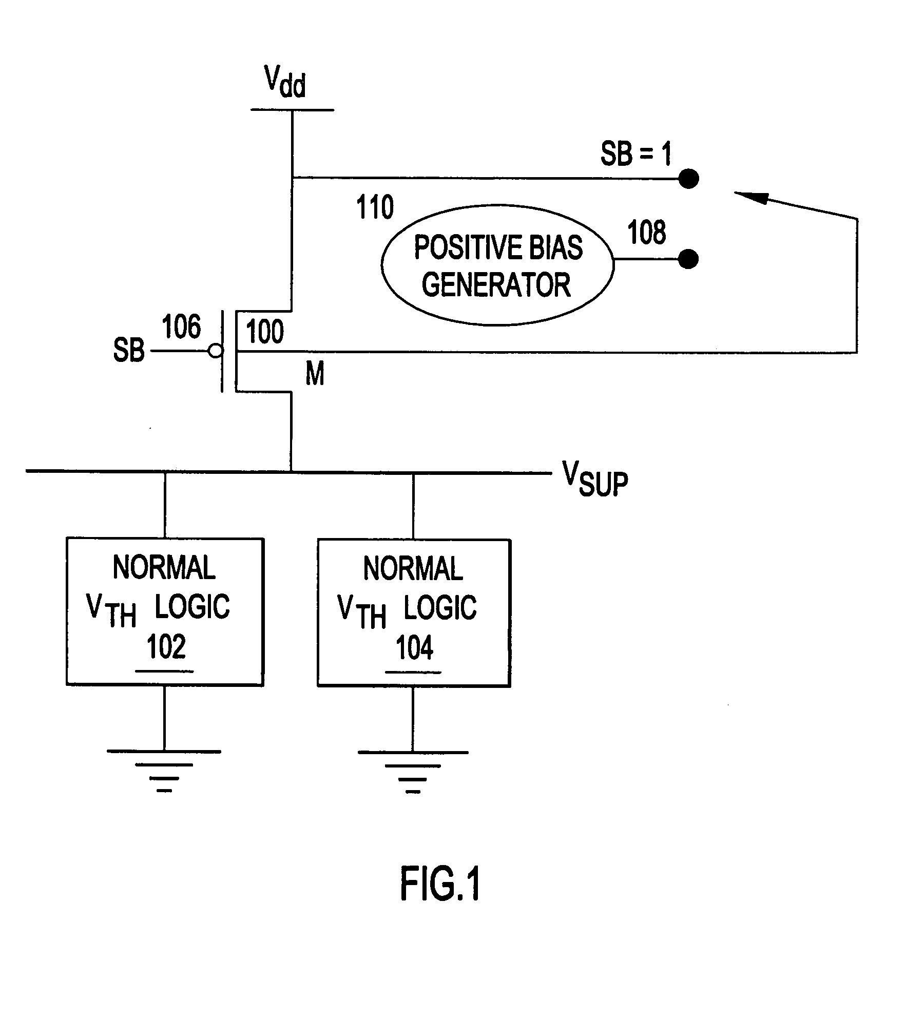
Turning now to the drawings and, more particularly, FIG. 1 shows a multi-threshold CMOS (MTCMOS) technology example of a preferred embodiment of the present invention, wherein supply switching devices 100 selectively alternately supply power and isolate logic circuits 102, 104. In this first example, switching devices 100 are field effect transistors (FETs) with higher thresholds than logic circuit FETs. It should be noted that as used herein, high threshold or higher threshold devices refers to devices with process features included to increase the magnitude of device threshold above base process devices, e.g., with thicker gate oxide, extra implants and etc. Further, it is understood that although an example may be directed to a particular device type, whether p-type header or n-type footer, this is for example only and not intended as a limitation.

So, in this example the switching or header devices 100 are p-type FETs (PFETs) with higher threshold voltages than PFETs in logic ...


PUM


Abstract

A multi-threshold integrated circuit (IC) with reduced subthreshold leakage and method of reducing leakage. Selectable supply switching devices (NFETs and/or PFETS) between a logic circuit and supply connections (Vdd and Ground) for the circuit have higher thresholds than normal circuit devices. Some devices may have thresholds lowered when the supply switching devices are on. Header/footer devices with further higher threshold voltages and widths may be used to further increase off resistance and maintain/reduce on resistance. Alternatively, high threshold devices may be stacked to further reduce leakage to a point achieved for an even higher threshold. Intermediate supply connects at the devices may have decoupling capacitance and devices may be tapered for optimum stack height and an optimum taper ratio to minimize circuit leakage and circuit delay.

Description

BACKGROUND OF THE INVENTION 1. Field of the Invention The present invention is related to integrated circuit power consumption and more particularly to reducing static random access memory (SRAM) power consumption. 2. Background Description Semiconductor technology and chip manufacturing advances have resulted in a steady decrease of chip feature size to increase on-chip circuit switching frequency (circuit performance) and the number of transistors (circuit density). Generally, all other factors being constant, the active power consumed by a given unit increases linearly with switching frequency. Thus, not withstanding the decrease of chip supply voltage, chip power consumption has increased as well. Both at the chip and system levels, cooling and packaging costs have escalated as a natural result of this increase in chip power. For low end systems (e.g., handhelds, portable and mobile systems), where battery life is crucial, reducing net power consumption is important but, suc...

Claims


Application Information

Patent Timeline
IPC IPC(8): H03K19/00
CPCH03K19/0016
Inventor BROWN, RICHARD B.CHUANG, CHING-TE K.COOK, PETER W.DAS, KOUSHIK K.JOSHI, RAJIV V.
Owner GLOBALFOUNDRIES US INC
Why Eureka
Try Eureka