

Power chip stacking and packaging structure
A packaging structure and power chip technology, which is applied to semiconductor/solid-state device parts, semiconductor devices, electrical components, etc., can solve the problems of large packaging structure size, difficult chip interconnection electrodes, poor heat dissipation performance, etc., to achieve Excellent heat dissipation performance, wide application range, size reduction effect
- Summary
- Abstract
- Description
- Claims
- Application Information
AI Technical Summary
Problems solved by technology
Method used
Image

Examples
Embodiment approach 1
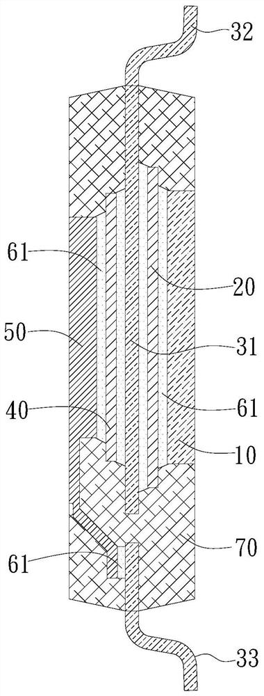
[0067] Embodiment 1: the first chip 20 is a triode chip, and the second chip 40 is a diode chip; the opposite sides of the triode are respectively provided with a source 21 and a drain, and the opposite sides of the diode chip are respectively provided with an anode and a cathode 41; the first electrode is the source 21, the second electrode is the drain, the third electrode is the cathode 41, and the fourth electrode is the anode.
[0068] When the power chip stack package structure is applied, in the circuit between the triode chip and the circuit board 80, the diode chip is connected in parallel, and the drain of the triode chip is connected to the cathode 41 of the diode chip, and the reverse current can be cut off through the diode chip.
[0069] In this embodiment, the triode chip is used as the first chip 20. In this way, the source 21 is welded to the metal sheet 10. In application, the metal sheet 10 can be directly welded to the circuit board 80 to realize the connect...
Embodiment approach 2
[0071] Embodiment 2: the first chip 20 is a diode chip, and the second chip 40 is a triode chip; the opposite sides of the triode are respectively provided with a source 21 and a drain, and the opposite sides of the diode chip are respectively provided with an anode and a cathode 41; the first electrode is an anode, the second electrode is a cathode 41 , the third electrode is a drain, and the fourth electrode is a source 21 .
[0072] The triode chip mentioned in the present invention may be, but not limited to, a MOSFET chip; the triode chip is a switching device.
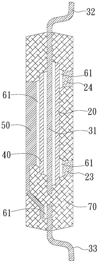
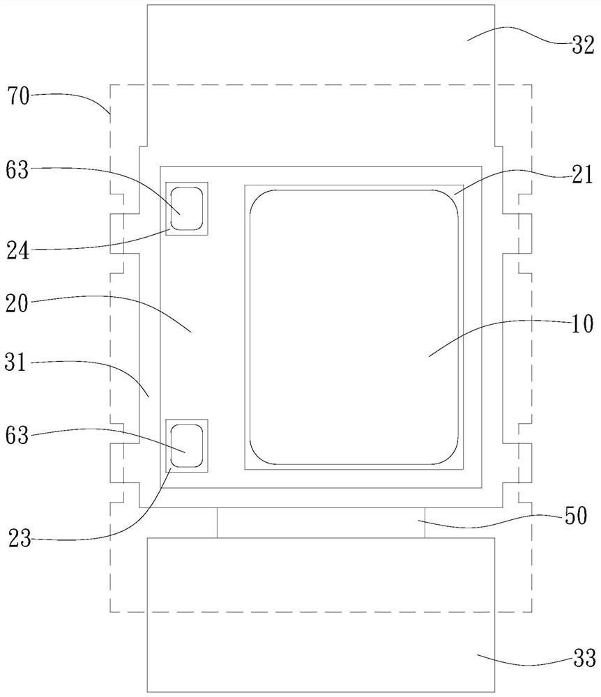
[0073] In one embodiment, the first chip 20 is a triode chip, the first electrode is the source 21, and the second electrode is the drain; the first chip 20 also includes a gate 23 coplanar with the source 21;
[0074] The lead frame also includes a third pin 34 insulated from the base island 31, and the gate 23 is electrically connected to the third pin 34 through a metal wire 62; or, the power chip stack packa...
PUM
 Abstract
Description
Claims
Application Information