Three-level circuit silicon carbide power module

A power module and three-level technology, which is applied to circuits, circuit layout on insulating boards, and circuit layout on support structures, can solve the problems of uneven current flow and low power density of switching tubes, and reduce parasitic inductance of loops , improve performance and reliability, and avoid the effect of volume increase

Pending Publication Date: 2021-04-23
HUAZHONG UNIV OF SCI & TECH
View PDF0 Cites 3 Cited by
  • Summary
  • Abstract
  • Description
  • Claims
  • Application Information

AI Technical Summary

Problems solved by technology

[0006] In view of the defects of the prior art, the purpose of the present invention is to provide a three-level circuit silicon carbide power module, which aims to solve the problems of parasitic inductance, uneven current of switching tubes and low power density existing in the existing three-level power module

Method used


Image

  • Three-level circuit silicon carbide power module
  • Three-level circuit silicon carbide power module
  • Three-level circuit silicon carbide power module

Examples


Embodiment

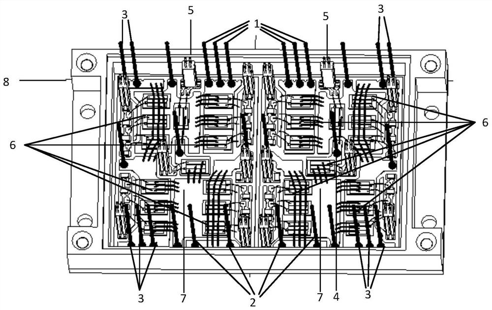
[0027] figure 1 It shows the structural diagram of the three-level full-bridge silicon carbide power module provided in this example, which includes positive power terminal 1, negative power terminal 2, AC output power terminal 3, neutral point power terminal 4, and drive terminal 5 , a silicon carbide power chip 6 , a DBC substrate 7 , a bottom plate, and a packaging shell 8 . Among them, the silicon carbide power chips 6 constitute two ANPC half-bridge power circuits, which are welded on the DBC substrate 7 , and the power terminals are connected to the DBC substrate 7 .

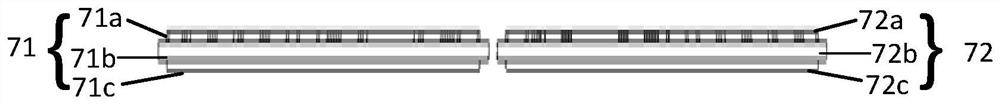
[0028] figure 2 A structural diagram of the DBC substrate of this example is shown, including a first DBC substrate 71 and a second DBC substrate 72 . The first DBC substrate 71 includes a first heat dissipation layer 71c, a first insulating layer 71b and a first circuit layer 71a; the second DBC substrate 72 includes a second heat dissipation layer 72c, a second insulating layer 72b and a second circui...


PUM


Abstract

The invention discloses a three-level circuit silicon carbide power module, and belongs to the technical field of power electronics. The power module comprises: a bottom layer direct copper-clad ceramic DBC substrate; and silicon carbide power chips, a driving resistor, a power terminal and a driving terminal which are welded on the bottom layer DBC substrate. Thesilicon carbide power chip and the driving resistorform a three-level full-bridge circuit; the silicon carbide power chips are connected through metal bonding wires; and the bottom layer directcopper-coated ceramic DBC substrate is welded to a bottom plate. According to the power module provided by the invention, through reasonable DBC copper layer layout, a current conversion loop is optimized, the balance of a parallel chip loop is realized, the parasitic inductance of the loop is greatly reduced, the size of the module is reduced, and the power density of the module is improved.

Description

technical field [0001] The invention belongs to the technical field of power electronics, and more specifically relates to a silicon carbide power module with a three-level circuit. Background technique [0002] Power electronics technology is widely used in many fields such as aerospace, rail transit, electric vehicles and power systems. With the development of high-power power electronic devices, PWM converters are developing from two-level converters to multi-level converters, especially three-level converters. [0003] In order to make the structure of the power electronic device more compact and reduce the volume, multiple power electronic devices and necessary auxiliary components are often made into modules. At present, the power devices used in the commercial three-level power modules that have appeared on the market are still mainly silicon devices, which cannot effectively increase the power density of the modules. The use of new wide-bandgap semiconductor power ...

Claims


Application Information

Patent Timeline
Patent Type & Authority Applications(China)
IPC IPC(8): H01L25/07H01L23/535H05K7/06
CPCH01L25/072H01L23/5386H05K7/06H01L2224/4903H01L2224/49111H01L2924/19107
Inventor 陈材王志伟郭心悦黄志召刘新民康勇
Owner HUAZHONG UNIV OF SCI & TECH
Why Eureka
Try Eureka