Micro-LED display with integrated structure and preparation method thereof

A display and p-gan technology, applied in semiconductor/solid-state device manufacturing, semiconductor devices, electric solid-state devices, etc., can solve problems affecting LED optoelectronic performance, low epitaxial layer crystal quality, large thermal mismatch and lattice mismatch, etc. problems, to achieve the effect of improving light extraction efficiency, simplifying the process, and making the preparation process mature

Active Publication Date: 2021-04-23
贵溪穿越光电科技有限公司
View PDF5 Cites 5 Cited by
  • Summary
  • Abstract
  • Description
  • Claims
  • Application Information

AI Technical Summary

Problems solved by technology

In this method, due to the large thermal mismatch and lattice mismatch between GaN and Si substrates, the crystal quality of the epitaxial layer is low, which affects the optoelectronic performance of the LED.

Method used


Image

  • Micro-LED display with integrated structure and preparation method thereof
  • Micro-LED display with integrated structure and preparation method thereof
  • Micro-LED display with integrated structure and preparation method thereof

Examples


Embodiment

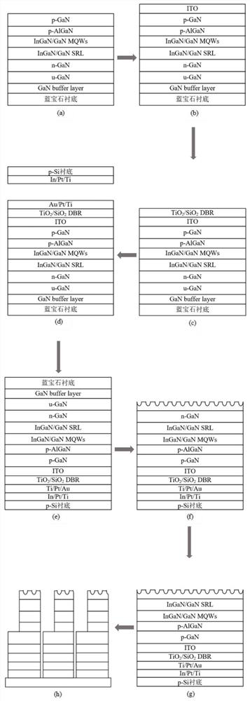
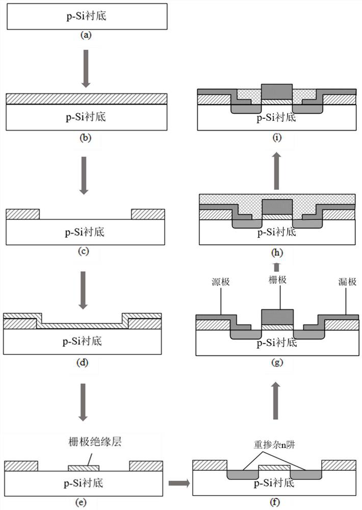
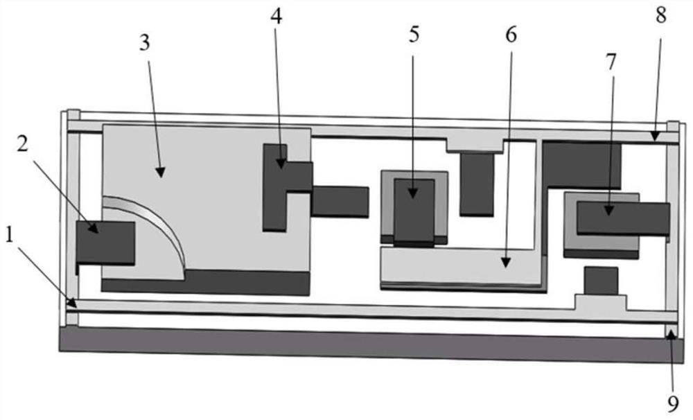
[0054] The present invention provides a method for manufacturing an integrated structure of a Micro-LED display, which specifically includes the following steps:

[0055] (1) Put the cleaned c-plane patterned (with hemispherical micro-nano structure) sapphire substrate into the MOCVD equipment.

[0056] (2) Growth of epitaxial layer

[0057] S1. A 20nm-thick low-temperature GaN buffer layer (GaN buffer layer) is grown at a temperature of 530°C.

[0058] S2. Under the condition of a temperature of 1025° C., a layer of 3 μm thick undoped GaN layer (u-GaN) is grown.

[0059] S3. At a temperature of 1025°C, grow a 2.5um thick Si-doped n-GaN layer with a Si doping concentration of 5×10 18 cm -3 .

[0060] S4. Under the condition of 820° C., grow an InGaN / GaN superlattice stress relief layer (InGaN / GaNSRL) with a thickness of 200 nm.

[0061] S5. Growth 12 cycles In 0.16 Ga 0.84 N / GaN multiple quantum wells (GaN MQWs), where In 0.16 Ga 0.84 The thickness of the N layer is 3...


PUM

PropertyMeasurementUnit
thicknessaaaaaaaaaa
thicknessaaaaaaaaaa
thicknessaaaaaaaaaa

Abstract

The invention discloses a Micro-LED display with an integrated structure and a preparation method thereof. The Micro-LED display comprises a Micro-LED chip array, and a chip comprises a p-Si substrate, a Micro-LED body, two transistors and a capacitor, wherein the Micro-LED body is of a step structure and comprises a bonding metal layer, a TiO2 / SiO2 DBR, an ITO layer, an Mg-doped p-GaN layer, an Mg-doped p-AlGaN electronic barrier layer, an InGaN / GaN multi-quantum well layer, an InGaN / GaN superlattice stress release layer and a surface-roughened Si-doped n-GaN layer from bottom to top, the upper surface of the Mg-doped p-GaN layer is a step surface, and the body is connected with the substrate through the bonding metal layer. According to the structure, active driving can be realized without transfer of a large number of Micro-LEDs, the crystal quality of the GaN epitaxial layer is improved, and the photoelectric performance of the Micro-LED is improved.

Description

technical field [0001] The invention belongs to the field of semiconductor devices, and in particular relates to an integrated structure Micro-LED display and a preparation method thereof. Background technique [0002] Currently, gallium nitride-based diodes are mainly used in lighting and displays. In the field of display, Micro-LED has higher luminous efficiency, higher contrast ratio and higher energy efficiency than mainstream technologies based on LCD or OLED. Because Micro-LED has these advantages, it can be applied to wearable devices, head-up displays, and high-resolution displays, and has broad application prospects. [0003] There are two main ways to drive Micro-LEDs: active drive (AM) and passive drive (PM). In active driving, a Micro-LED driving circuit requires at least two transistors and a capacitor, and its structure is more complicated than that of passive driving. However, compared with passive drivers, active drivers have many advantages such as strong...

Claims


Application Information

Patent Timeline
Patent Type & Authority Applications(China)
IPC IPC(8): H01L27/15H01L21/77H01L33/32H01L33/46H01L33/22
CPCH01L27/156H01L21/77H01L33/32H01L33/46H01L33/22
Inventor 周圣军杜鹏雷宇
Owner 贵溪穿越光电科技有限公司
Why Eureka
Try Eureka