Perovskite solar cell device and packaging method thereof
A technology of solar cells and packaging methods, applied in the direction of electric solid devices, electrical components, semiconductor devices, etc., can solve problems such as poor stability, and achieve the effects of overcoming poor stability, reducing damage, and inhibiting decomposition reactions
- Summary
- Abstract
- Description
- Claims
- Application Information
AI Technical Summary
Problems solved by technology
Method used
Image
Examples
specific Embodiment 1
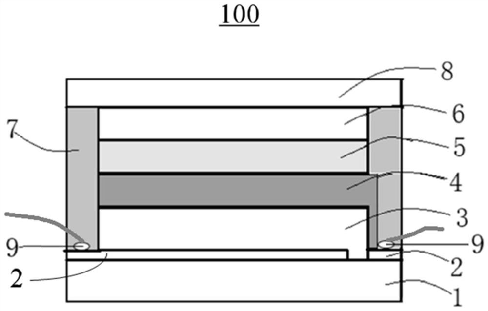
[0076] (1) Prepare perovskite solar cells on transparent conductive glass. The structure of the cell adopts the pin type trans structure "transparent conductive layer / hole transport layer / perovskite / electron transport layer / buffer layer / metal electrode" FTO / NiO / FA 0.85 Cs 0.15 Pb(I 0.95 Br 0.05 ) 3 / PCBM / BCP / Ag structure.
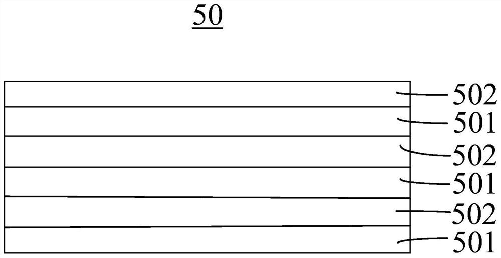
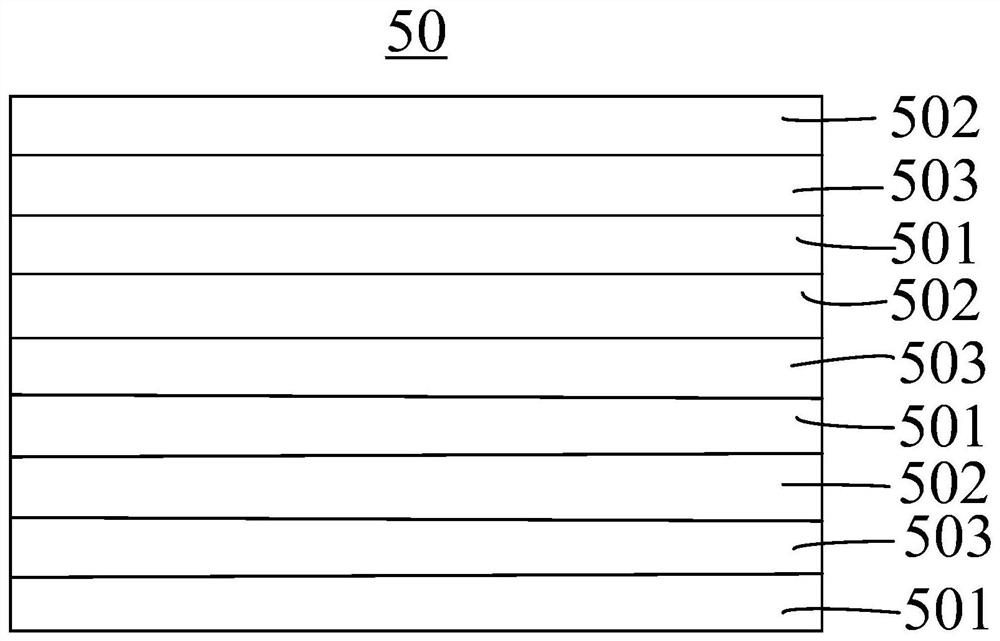
[0077] (2) The cover plate is hot-pressed and packaged (there is a cavity structure between the cover plate and the battery), and a layer of Pyraline C with a thickness of 300nm is deposited first, and then the cover plate is hot-pressed and bonded without gaps (note: the cover plate There is no cavity structure between the board and the Paralyne C film layer), sequentially deposit a layer of 300nm thick Paralyne C / evaporate a layer of 50nm thick MgF 2 / Deposit a layer of 40nm-thick aluminum oxide back cover plate hot-pressed gap-free bonding package (note: there is no cavity structure between the cover plate and the aluminum oxide film layer), seque...
specific Embodiment 2
[0084] (1) Prepare perovskite solar cells on transparent conductive glass. The structure of the cell adopts the pin type trans structure "transparent conductive layer / hole transport layer / perovskite / electron transport layer / buffer layer / metal electrode" FTO / NiO / FA 0.85 Cs 0.15 Pb(I 0.95 Br 0.05 ) 3 / PCBM / BCP / Ag structure.
[0085] (2) Use UV glue cover plate for gap-free bonding package, first deposit a layer of 300nm-thick Paralin C, then UV glue cover plate for gap-free bonding package, and then deposit a layer of 300nm-thick Paraline C / Evaporate a layer of 50nm thick MgF 2 / After depositing a layer of 40nm thick aluminum oxide, the UV glue cover plate is bonded and packaged without gaps, and sequentially deposits a layer of 300nm thick paraffin C / evaporates a layer of 50nm thick MgF 2 / Deposit a layer of 40nm thick aluminum oxide as a multi-layer thin film packaging method to prepare perovskite solar cell devices. Pay attention to the lead-out part of the prote...
specific Embodiment 3
[0089] (1) Prepare perovskite solar cells on transparent conductive glass. The structure of the cell adopts the pin type trans structure "transparent conductive layer / hole transport layer / perovskite / electron transport layer / buffer layer / metal electrode" FTO / NiO / FA 0.85 Cs 0.15 Pb(I 0.95 Br 0.05 ) 3 / PCBM / BCP / Ag structure.
[0090] (2) On the surface of the battery, first use chemical vapor deposition of 300nm thick Paralin C, and then evaporate a layer of 50nm thick MgF 2 Increase its surface wettability, and finally use ALD to deposit a layer of aluminum oxide to form an inert barrier film package. Pay attention to the lead-out part of the protective electrode wire, and it cannot be covered by the inert layer to affect the subsequent charge export.
[0091] (3) After the film is packaged, the cover plate is bonded and packaged without gaps. The glass cover plate is tightly bonded to the battery plate through ultraviolet curing glue, and after being cured by ultraviolet...
PUM
| Property | Measurement | Unit |
|---|---|---|
| thickness | aaaaa | aaaaa |
| thickness | aaaaa | aaaaa |
| thickness | aaaaa | aaaaa |
Abstract
Description
Claims
Application Information
 - R&D
- Intellectual Property
- Life Sciences
- Materials
- Tech Scout
- Unparalleled Data Quality
- Higher Quality Content
- 60% Fewer Hallucinations
Browse by: Latest US Patents, China's latest patents, Technical Efficacy Thesaurus, Application Domain, Technology Topic, Popular Technical Reports.
© 2025 PatSnap. All rights reserved.Legal|Privacy policy|Modern Slavery Act Transparency Statement|Sitemap|About US| Contact US: help@patsnap.com


