Light-emitting diode with variable pattern and preparation method thereof

A technology of light-emitting diodes and diodes, which is applied in the field of optoelectronics, can solve the problems of low utilization rate of light sources, and achieve the effects of reasonable step design, high practicability, and simple structure

Active Publication Date: 2021-05-04
SHANDONG INSPUR HUAGUANG OPTOELECTRONICS
View PDF4 Cites 3 Cited by
  • Summary
  • Abstract
  • Description
  • Claims
  • Application Information

AI Technical Summary

Problems solved by technology

However, since most of the light emitted by the light source is blocked by the reticle, only a small amount of light is emitted, so the utilization rate of the light source is low.

Method used


Image

  • Light-emitting diode with variable pattern and preparation method thereof
  • Light-emitting diode with variable pattern and preparation method thereof
  • Light-emitting diode with variable pattern and preparation method thereof

Examples


Embodiment 1

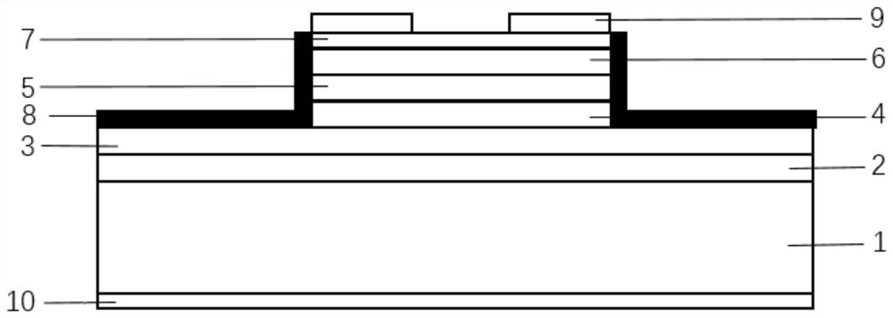
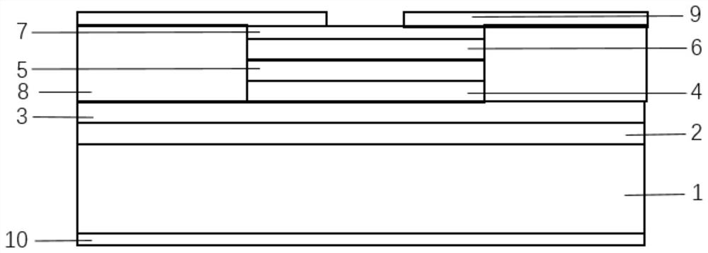
[0051] S1: Take substrate 1, grow N-type ohmic contact layer 2, N-type confinement layer 3, active region 4, P-type confinement layer 5 and P-type ohmic contact layer 6 sequentially on the surface of substrate 1 by MOCVD method to obtain epitaxy piece;

[0052] S2: Place the epitaxial wafer with the N side down and the P side up in the electron beam evaporation table, and evaporate the ITO film 7 on the P-type ohmic contact layer 6, and the ITO film 7 covers the entire surface of the epitaxial wafer; the thickness of the ITO film 7 is

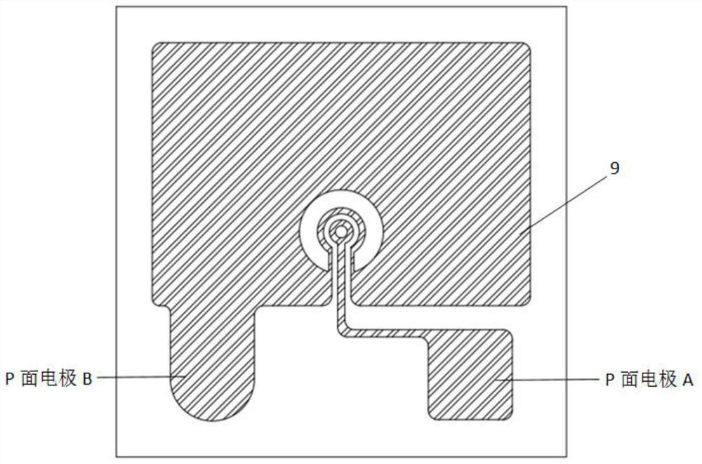
[0053] S3: Place the epitaxial wafer P on the suction cup of the coating machine, coat the photoresist, expose the light-emitting pattern of the light-emitting area A, and the light-emitting pattern of the light-emitting area B; then develop and etch, at this time on the surface of the ITO film 7 forming a light emitting region A and a light emitting region B, and the surfaces of the light emitting region A and the light emitting region B are...

Embodiment 2

[0062] S1: Take substrate 1, grow N-type ohmic contact layer 2, N-type confinement layer 3, active region 4, P-type confinement layer 5 and P-type ohmic contact layer 6 sequentially on the surface of substrate 1 by MOCVD method to obtain epitaxy piece;

[0063] S2: Place the epitaxial wafer with the N side down and the P side up in the electron beam evaporation table, and evaporate the ITO film 7 on the P-type ohmic contact layer 6, and the ITO film 7 covers the entire surface of the epitaxial wafer; the thickness of the ITO film 7 is

[0064] S3: Place the epitaxial wafer P on the suction cup of the coating machine, coat the photoresist, expose the light-emitting pattern of the light-emitting area A, and the light-emitting pattern of the light-emitting area B; then develop and etch, at this time on the surface of the ITO film 7 forming a light emitting region A and a light emitting region B, and the surfaces of the light emitting region A and the light emitting region B are...

Embodiment 3

[0073] S1: Take substrate 1, grow N-type ohmic contact layer 2, N-type confinement layer 3, active region 4, P-type confinement layer 5 and P-type ohmic contact layer 6 sequentially on the surface of substrate 1 by MOCVD method to obtain epitaxy piece;

[0074] S2: Place the epitaxial wafer with the N side down and the P side up in the electron beam evaporation table, and evaporate the ITO film 7 on the P-type ohmic contact layer 6, and the ITO film 7 covers the entire surface of the epitaxial wafer; the thickness of the ITO film 7 is

[0075] S3: Place the epitaxial wafer P on the suction cup of the coating machine, coat the photoresist, expose the light-emitting pattern of the light-emitting area A, and the light-emitting pattern of the light-emitting area B; then develop and etch, at this time on the surface of the ITO film 7 forming a light emitting region A and a light emitting region B, and the surfaces of the light emitting region A and the light emitting region B are...


PUM


Abstract

The invention discloses a light-emitting diode with a variable pattern and a preparation method thereof. The diode comprises an epitaxial wafer, wherein an ITO film is evaporated on the upper surface of the epitaxial wafer, the ITO film is provided with a plurality of light-emitting areas and etching areas, each light-emitting area is correspondingly provided with a P-surface electrode, the adjacent P-surface electrodes are insulated and separated, an insulating layer is deposited on the surface of each etching area, and an N-face electrode is evaporated on the end face of the side, away from the ITO film, of the epitaxial wafer. The method is simple in structure and reasonable in step design, the prepared light-emitting diode can be used independently, does not need to work in cooperation with a reticle and can emit needed patterns, and the advantages of simple structure and low power consumption are guaranteed while the utilization rate of a light source is improved; and meanwhile, the luminous pattern of the diode prepared by using the technical scheme has variability, and can be changed according to a distance between a reflection sighting telescope and a target, and the practicability of the diode is relatively high.

Description

technical field [0001] The invention relates to the technical field of optoelectronics, in particular to a light-emitting diode with variable patterns and a preparation method thereof. Background technique [0002] The reflective sight is a kind of optical sight without magnification. It uses the principle of spherical reflection to make the reflected light incident on the eyes parallel to the observer's eyes, so that the observer's eyes can be seen without being on the central axis of the lens. Seeing the red dot can improve shooting accuracy when moving targets or body movement. The light source part of the reflective sight currently includes LED / LD light source, isotope radiation light source and so on. [0003] The isotope radiation source uses the visible light radiated by a radioactive element as the light source. Although its lifespan is very long, the cost is relatively high. The LED / LD light source is to place a circular or other patterned reticle in front of the ...

Claims


Application Information

Patent Timeline
Patent Type & Authority Applications(China)
IPC IPC(8): H01L33/00H01L33/08H01L33/14H01L33/36F41G1/00
CPCF41G1/00H01L33/005H01L33/08H01L33/14H01L33/36H01L2933/0016
Inventor 吴向龙闫宝华汤福国王成新徐现刚
Owner SHANDONG INSPUR HUAGUANG OPTOELECTRONICS
Why Eureka
Try Eureka