A light-emitting diode with variable graphics and its preparation method
A technology of light-emitting diodes and diodes, applied in the field of optoelectronics, can solve the problems of low utilization rate of light sources, and achieve the effects of reasonable step design, high practicability and low power consumption
- Summary
- Abstract
- Description
- Claims
- Application Information
AI Technical Summary
Problems solved by technology
Method used
Image
Examples
Embodiment 1
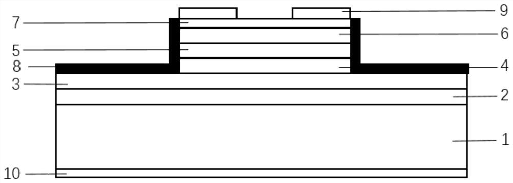
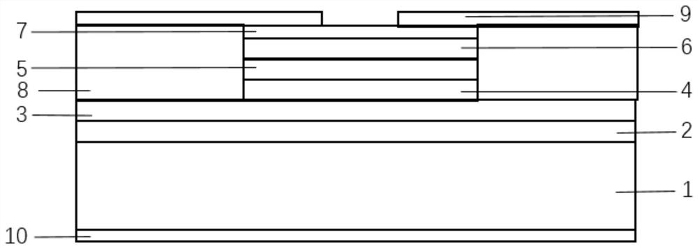
[0051] S1: Take substrate 1, grow N-type ohmic contact layer 2, N-type confinement layer 3, active region 4, P-type confinement layer 5 and P-type ohmic contact layer 6 sequentially on the surface of substrate 1 by MOCVD method to obtain epitaxy piece;
[0052] S2: Place the epitaxial wafer with the N side down and the P side up in the electron beam evaporation table, and evaporate the ITO film 7 on the P-type ohmic contact layer 6, and the ITO film 7 covers the entire surface of the epitaxial wafer; the thickness of the ITO film 7 is
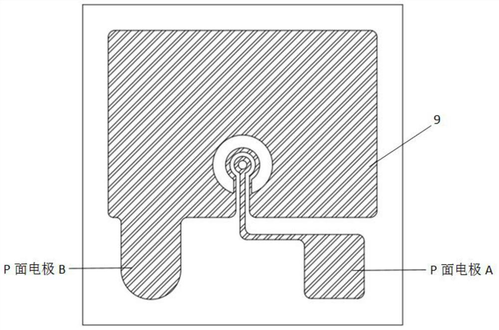
[0053] S3: Place the epitaxial wafer P on the suction cup of the coating machine, coat the photoresist, expose the light-emitting pattern of the light-emitting area A, and the light-emitting pattern of the light-emitting area B; then develop and etch, at this time on the surface of the ITO film 7 forming a light emitting region A and a light emitting region B, and the surfaces of the light emitting region A and the light emitting region B are...
Embodiment 2
[0062] S1: Take substrate 1, grow N-type ohmic contact layer 2, N-type confinement layer 3, active region 4, P-type confinement layer 5 and P-type ohmic contact layer 6 sequentially on the surface of substrate 1 by MOCVD method to obtain epitaxy piece;
[0063] S2: Place the epitaxial wafer with the N side down and the P side up in the electron beam evaporation table, and evaporate the ITO film 7 on the P-type ohmic contact layer 6, and the ITO film 7 covers the entire surface of the epitaxial wafer; the thickness of the ITO film 7 is
[0064] S3: Place the epitaxial wafer P on the suction cup of the coating machine, coat the photoresist, expose the light-emitting pattern of the light-emitting area A, and the light-emitting pattern of the light-emitting area B; then develop and etch, at this time on the surface of the ITO film 7 forming a light emitting region A and a light emitting region B, and the surfaces of the light emitting region A and the light emitting region B are...
Embodiment 3
[0073] S1: Take substrate 1, grow N-type ohmic contact layer 2, N-type confinement layer 3, active region 4, P-type confinement layer 5 and P-type ohmic contact layer 6 sequentially on the surface of substrate 1 by MOCVD method to obtain epitaxy piece;
[0074] S2: Place the epitaxial wafer with the N side down and the P side up in the electron beam evaporation table, and evaporate the ITO film 7 on the P-type ohmic contact layer 6, and the ITO film 7 covers the entire surface of the epitaxial wafer; the thickness of the ITO film 7 is
[0075] S3: Place the epitaxial wafer P on the suction cup of the coating machine, coat the photoresist, expose the light-emitting pattern of the light-emitting area A, and the light-emitting pattern of the light-emitting area B; then develop and etch, at this time on the surface of the ITO film 7 forming a light emitting region A and a light emitting region B, and the surfaces of the light emitting region A and the light emitting region B are...
PUM
 Abstract
Description
Claims
Application Information


