Light emitting diode and manufacturing method thereof
A technology of light-emitting diodes and light-emitting units, which is applied in semiconductor/solid-state device manufacturing, electrical components, and electrical solid-state devices, etc., can solve the problems of poor heat dissipation, low thrust, and small electrode area.
- Summary
- Abstract
- Description
- Claims
- Application Information
AI Technical Summary
Problems solved by technology
Method used
Image

Examples
Embodiment 1
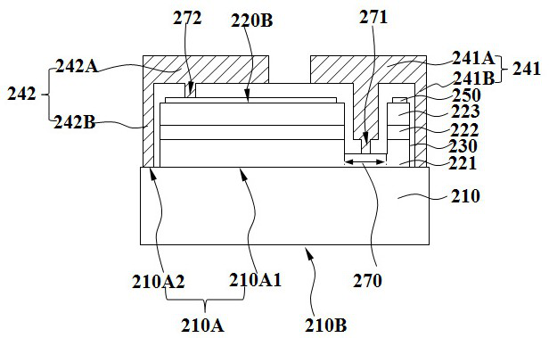
[0034] This embodiment discloses the following flip-chip LED chip, as shown in Figure 1(a), which includes the following stacked layers: a transparent substrate 210, a light-emitting epitaxial stack, an insulating layer 230, a first electrode 241 and a second electrode. Two electrodes 242 . The LED chip can be a small-sized LED chip with a smaller horizontal area, for example, it can have a thickness of about 62500 μm 2 The following horizontal cross-sectional area, which in turn can have about 900μm 2 Above and about 62500μm 2 The horizontal cross-sectional area below. For example, the LED chip may have dimensions of 230 μm×120 μm or 120 μm×80 μm or 100 μm×60 μm or 50 μm×40 μm. However, the horizontal length and vertical length of the LE chip in the embodiment are not limited to the above content.
[0035] The details of each structural stack layer are described below.
[0036] Wherein, as shown in FIG. 1(a), the transparent substrate 210 may be a growth substrate for th...
Embodiment 2
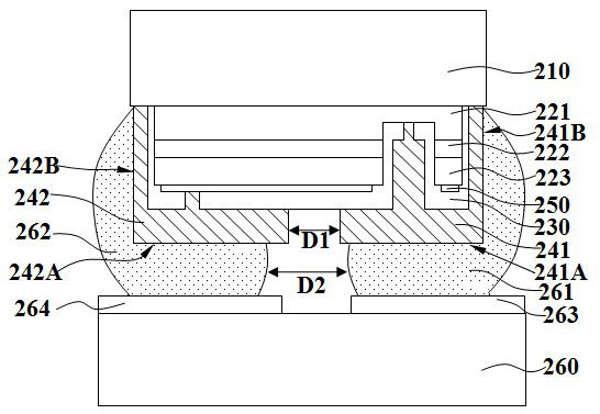
[0058] image 3 and Figure 4 Another flip-chip LED chip implemented in accordance with the present invention is shown. Different from Embodiment 1, the outer periphery of the first surface 210A of the transparent substrate 210 has a step 211, and the step 211 has a third surface 210D between the first surface 210A and the second surface 210B, and connects the first The side wall 210E of the surface and the third surface, the first electrode 241A and / or the second electrode 242 extend to the step 211, at least partially covering the side wall 210E and the third surface connecting the first surface and the third surface 210D. The distance from the third surface 210D to the first surface 210A is preferably 10-40 μm, such as 20-30 μm, and the distance from the third surface to the second surface is preferably 10-60 μm, such as 30-50 μm. By providing a step 211 on the outer periphery of the transparent substrate 210 and extending the first electrode and / or the second electrode ...
Embodiment 3
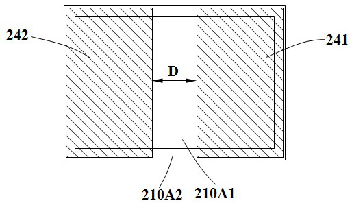
[0071] In the LED chip supported by a transparent substrate, after the transparent substrate is thinned, the LED chip is usually cut by means of implicit cutting and splitting. For an approximately 62500µm 2 A small-sized LED chip with a horizontal cross-sectional area below, for example, an LED chip can have a size of 230 μm×120 μm or 120 μm×80 μm or 100 μm×60 μm or 50 μm×40 μm. The size of the remaining cutting track is limited, and the cutting edge distortion and even cutting edge chipping often occur during the splitting process. Figure 11 It shows a kind of hidden cutting and splitting formation Figure 31 The physical photo map of the LED chip shown. The gray and white part 110A1 of each LED chip is the surface of the transparent substrate exposed around the light-emitting mesa 120 in the LED chip. This area reserves a cutting line with a certain width for cutting processes such as laser hidden cutting and splitting. The cutting line passes through the cutting process....
PUM
| Property | Measurement | Unit |
|---|---|---|
| Thickness | aaaaa | aaaaa |
| Side length | aaaaa | aaaaa |
| Thickness | aaaaa | aaaaa |
Abstract
Description
Claims
Application Information
 - R&D
- Intellectual Property
- Life Sciences
- Materials
- Tech Scout
- Unparalleled Data Quality
- Higher Quality Content
- 60% Fewer Hallucinations
Browse by: Latest US Patents, China's latest patents, Technical Efficacy Thesaurus, Application Domain, Technology Topic, Popular Technical Reports.
© 2025 PatSnap. All rights reserved.Legal|Privacy policy|Modern Slavery Act Transparency Statement|Sitemap|About US| Contact US: help@patsnap.com