Self-excited drive and power conversion circuit based on gan HEMT device
A technology for converting circuits and power, applied in the direction of converting DC power input to DC power output, output power conversion devices, instruments, etc., can solve the problems of unfavorable product power density, large junction capacitance, etc., and achieve the expansion of application power level and reduction The effect of small size and reduced system application cost
- Summary
- Abstract
- Description
- Claims
- Application Information
AI Technical Summary
Problems solved by technology
Method used
Image
Examples
Embodiment 1
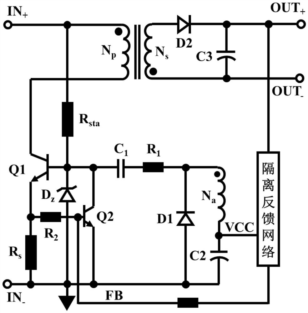
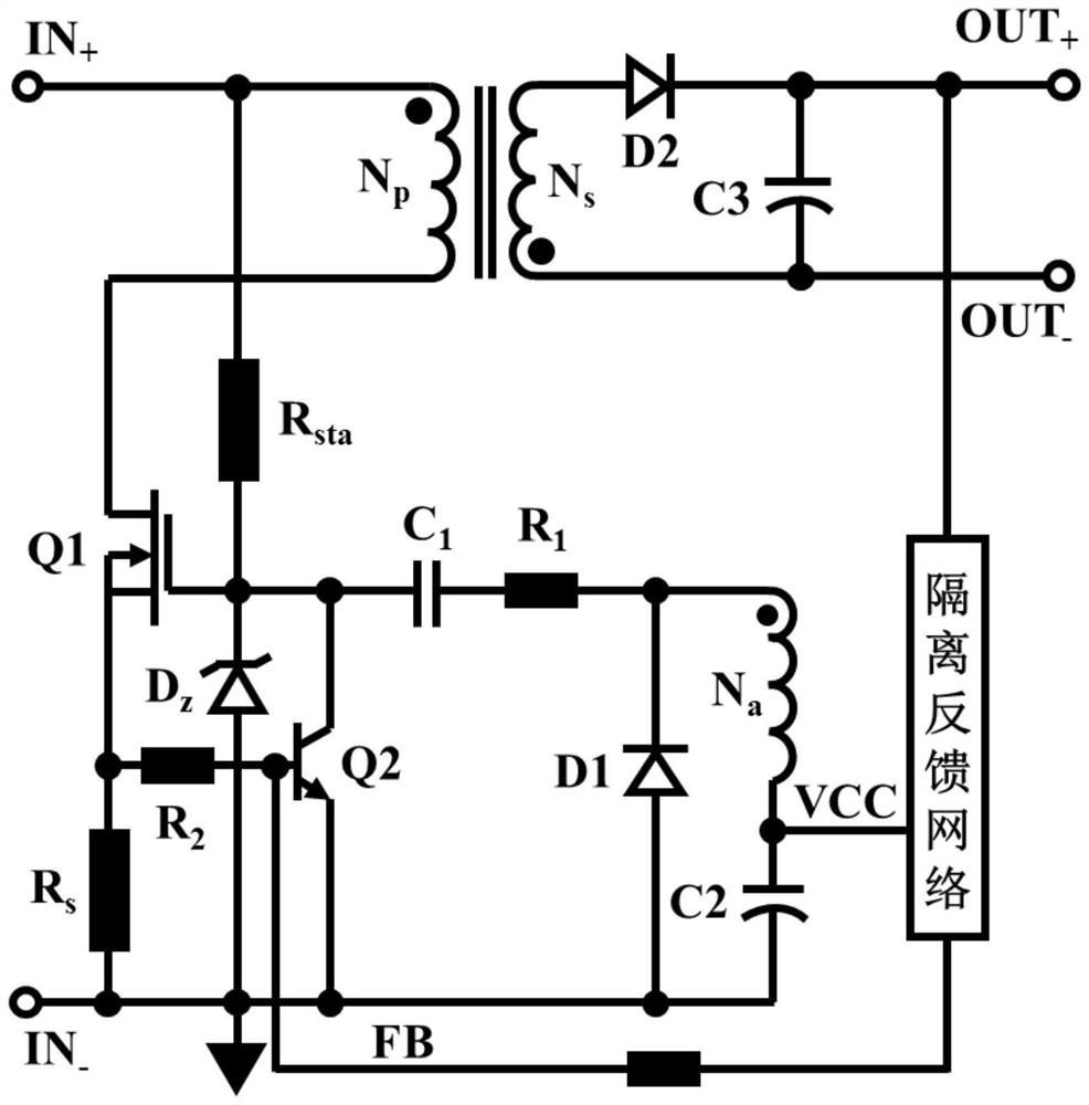
[0036] This self-excited drive and power conversion circuit based on GaN HEMT devices includes: start-up circuit, power conversion circuit, protection circuit, Zener diode Dz1, isolated feedback network, self-excited drive and cycle-by-cycle current detection circuit, drive buffer, output rectifier circuit;
[0037] The start-up circuit is composed of a resistor Rsta, one end is connected to the positive line of the power input, and the other end is connected to the cathode of the Zener diode Dz1, Rsta is the high-voltage start-up resistor of Q1, generally set to 680kΩ-3MΩ;
[0038] The power conversion circuit is composed of the winding Np of the transformer, the main power tube Q1 and the feedback function tube Q2. Q1 is an enhanced GaN HEMT device, the gate of which is connected to the cathode of the Zener diode Dz1, and the source is connected to the anode of the Zener diode Dz1. And grounded, the terminal with the same name of the winding Np is connected to the input posi...
Embodiment 2
[0049] The structure of this embodiment is basically the same as that of Embodiment 1, the difference is that the drive buffer includes resistors R101, R102, R103, R104, R106, NOT gates U101A, U101C, U101D, DC blocking capacitors C101, C102, Zener diodes Dz101, Dz102, and C1 pass the driving signal to the NOT gate U101A after being divided by R101, R102. After the level is reversed, it first passes through the voltage regulator and filter network DZ101, R103, and C101, and then passes through DZ102, R104, and C102 to the next Level NOT gates U101C, U101D, the level is reversed twice and then passed to the gate of Q1 through the resistor R106. The drive buffer generates inverting input and output logic, such as outputting a low level when the input is high.
[0050] The non-inverting and inverting outputs can also be integrated into the same driver buffer, and users can choose to connect according to their needs.
PUM
 Abstract
Description
Claims
Application Information


