Transmission electron microscope electrochemical detection chip and manufacturing method thereof

A transmission electron microscope and detection chip technology, applied in the direction of material electrochemical variables, measuring devices, scientific instruments, etc., can solve the problems of inconvenience, the electrochemical detection chip does not have the temperature detection function, etc., and achieve the effect of electric field stability

Pending Publication Date: 2021-06-04
XIAMEN UNIV
View PDF1 Cites 0 Cited by
  • Summary
  • Abstract
  • Description
  • Claims
  • Application Information

AI Technical Summary

Problems solved by technology

[0003] Invention patent application CN110736760A discloses an electrochemical detection chip, which has several deficiencies, the most important of which is that the electrochemical detection chip does not have a temperature detection function, which is not convenient for users to understand electrochemical reactions Types of endothermic and exothermic reactions and the effect of temperature on electrochemical reactions

Method used


Image

  • Transmission electron microscope electrochemical detection chip and manufacturing method thereof
  • Transmission electron microscope electrochemical detection chip and manufacturing method thereof
  • Transmission electron microscope electrochemical detection chip and manufacturing method thereof

Examples


Embodiment 1

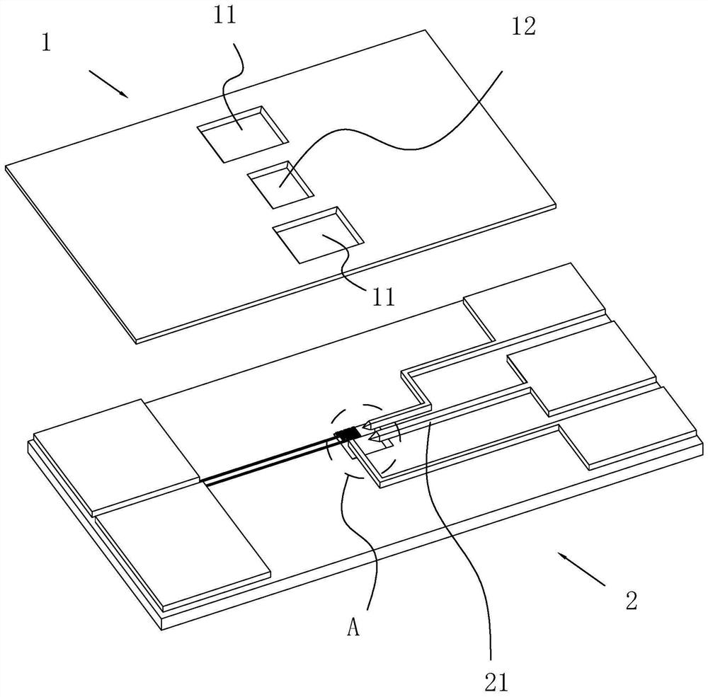
[0047] Such as Figures 1 to 4 As shown, a transmission electron microscope electrochemical detection chip includes an upper chip 1 and a lower chip 2, the upper chip 1 and the lower chip 2 are silicon substrates with insulating layers on the front and back sides.

[0048] Those skilled in the art are familiar with: the general structure of above-mentioned silicon substrate is as follows Figure 5 As shown, it includes a base silicon 31 in the middle, an insulating layer 32 on the front side and an insulating layer 33 on the back side. In this embodiment, the insulating layer is a silicon nitride layer or a silicon oxide layer, which prevents the reaction solution inside the chip from volatilizing and destroying the vacuum environment inside the electron microscope, and at the same time allows the electron beam to pass through to facilitate imaging by the transmission electron microscope. In this embodiment, the thickness of the insulating layer is 5-200 nanometers, and the t...

Embodiment 2

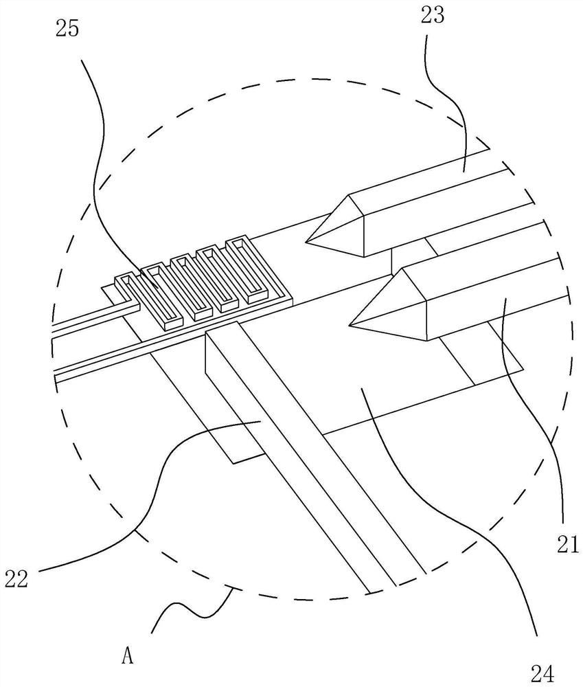
[0061] The difference between this embodiment and the first embodiment is that the TEM electrochemical detection chip also includes a carbon electrode (not shown in the figure), and the carbon electrode covers the working electrode 21 and is not in contact with the counter electrode 23 . The introduction of carbon electrodes can effectively improve imaging resolution and reduce background noise.

[0062] Further, the carbon electrode is composed of a carbon film plated on the working electrode 21, which is convenient for manufacture. In this embodiment, the thickness of the carbon film is 10-80 nanometers.

Embodiment 3

[0064] The present invention also provides a manufacturing method of a transmission electron microscope electrochemical detection chip, which can be used to manufacture the transmission electron microscope electrochemical detection chip described in Embodiment 1.

[0065] Such as Figure 6 As shown, the manufacturing method includes the following steps:

[0066] S1: Process the sample injection port and the first window on the silicon substrate A with insulating layers on both the front and back sides, and manufacture the top wafer.

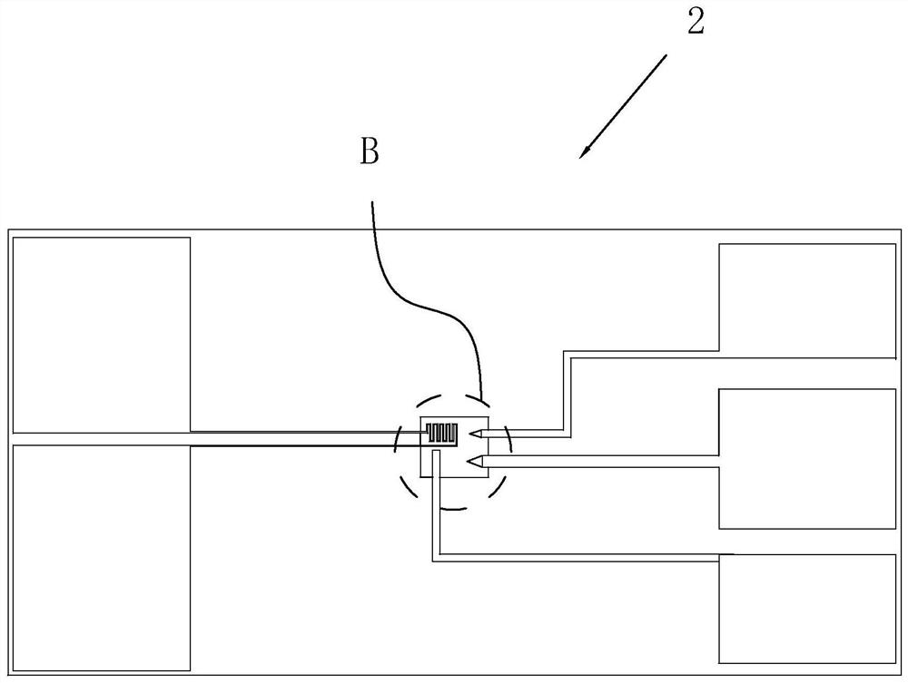
[0067] S2: Process a working electrode, a reference electrode, a counter electrode, a second window and a thermometer on the silicon substrate B with insulating layers on both the front and back sides, and manufacture the lower film.

[0068] S3: bonding the upper sheet and the lower sheet through an adhesive layer to obtain a transmission electron microscope electrochemical detection chip. The top sheet, bottom sheet, and adhesive layer togeth...


PUM

PropertyMeasurementUnit
thicknessaaaaaaaaaa
thicknessaaaaaaaaaa
thicknessaaaaaaaaaa

Abstract

The invention belongs to the technical field of electrochemical chips, and particularly relates to a transmission electron microscope electrochemical detection chip and a manufacturing method thereof. The transmission electron microscope electrochemical detection chip comprises an upper piece and a lower piece, the upper piece and the lower piece are both silicon substrates with insulating layers on the front and back surfaces, the front surface of the upper piece and the front surface of the lower piece are fixedly bonded through a bonding layer, and the upper piece, the lower piece and the bonding layer jointly form a cavity; and the upper piece is provided with a sample injection port and a first window, the lower piece is provided with a working electrode, a reference electrode, a counter electrode, a second window and a thermometer, and the working electrode, the reference electrode and the counter electrode are all arranged on the second window. The lower piece of the transmission electron microscope electrochemical detection chip provided by the invention is provided with the thermometer, and the thermometer can be used for monitoring the reaction temperature in real time, so that a user can better know the type of an electrochemical reaction heat absorption and release reaction and the influence of the temperature on the electrochemical reaction. The manufacturing method provided by the invention can be used for manufacturing the transmission electron microscope electrochemical detection chip.

Description

technical field [0001] The invention belongs to the technical field of electrochemical chips, and in particular relates to a transmission electron microscope electrochemical detection chip and a manufacturing method thereof. Background technique [0002] In the process of science and technology development, electrochemistry occupies an important position in the fields of electrolysis, electroplating, chemical power supply, electroanalysis, metal corrosion and protection. However, with the advancement of science and technology, the application range of electrochemistry has been expanded to the fields of environmental protection, electronics, energy, materials, chemical industry, metallurgy and chemical synthesis. Through the electrochemical detection chip of the transmission electron microscope, the redox process of metal atoms, organic molecules and other microscopic particles can be observed from a microscopic point of view. This information is very necessary for the analys...

Claims


Application Information

Patent Timeline
Patent Type & Authority Applications(China)
IPC IPC(8): G01N23/04G01N23/20058G01N23/20008G01N27/416G01N27/30
CPCG01N23/04G01N23/20008G01N23/20058G01N27/30G01N27/416
Inventor 廖洪钢邓俊先江友红
Owner XIAMEN UNIV
Why Eureka
Try Eureka