A wear-resistant and miscellaneous optical glass element and its preparation method and application
An optical glass, impurity-removing technology, applied in optical components, optics, instruments, etc., can solve the problems of limiting the wide application of optical glass, low wear resistance of optical glass, scratches of optical glass, etc., to improve wear resistance, The effect of enhancing strength and enriching the use environment
- Summary
- Abstract
- Description
- Claims
- Application Information
AI Technical Summary
Problems solved by technology
Method used
Image
Examples
preparation example Construction
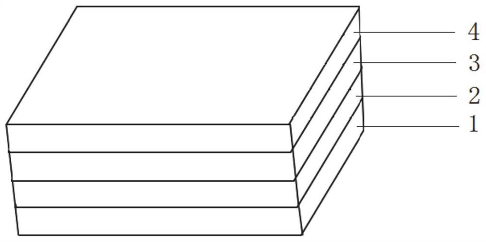
[0041] The second aspect of the present invention provides a method for preparing the above-mentioned wear-resistant and miscellaneous optical glass element, and the specific steps include:
[0042] (1) prepare glass compound, prepare optical glass matrix;
[0043] (2) introducing doped metal ions into the glass batch to form a mixture A, pouring it on the surface of the optical glass substrate, and performing a reduction treatment under a reducing gas atmosphere to form a base layer;
[0044] (3) introducing doped metal ions into the glass batch to form a mixture B, pouring it on the surface of the base layer, and performing a reduction treatment under a reducing gas atmosphere to form a transition layer;
[0045] (4) introducing doped metal ions into the glass batch to form a mixture C, pouring it on the surface of the transition layer, and performing a reduction treatment under a reducing gas atmosphere to form a functional layer;
[0046] (5) Post-processing the optical g...
Embodiment 1
[0056] (1) Prepare glass compound according to Table 1, prepare borosilicate K9 optical glass matrix;
[0057] (2) 0.05mol% TiO 2 and 3mol% SnO 2 Introduced into the glass batch to form a mixture A, poured on the surface of the optical glass substrate, in the H 2 Reduction at a temperature of 500°C for 10 hours, the pressure of the reduction treatment is 5MPa, and the base layer is formed, and the thickness of the base layer is 0.8mm;
[0058] (3) 1mol% TiO 2 and 3mol% SnO 2 Introduced into the glass batch to form the mixture B, poured on the surface of the base layer, in the H 2 Reduction at a temperature of 600°C for 20 hours, the pressure of the reduction treatment is 5MPa, and a transition layer is formed, and the thickness of the transition layer is 0.5mm;
[0059] (4) 10mol% TiO 2 and 3mol% SnO 2 Introduced into the glass batch to form a mixture C, poured on the surface of the transition layer, in the H 2 Reduction at a temperature of 700°C for 30 hours, the pres...
Embodiment 2
[0064] (1) Prepare glass compound according to Table 1, prepare borosilicate K9 optical glass matrix;
[0065] (2) 0.1mol% TiO 2 and 5mol% Ga 2 o 3 Introduced into the glass batch to form a mixture A, poured on the surface of the optical glass substrate, in the H 2 Reduction at a temperature of 550°C for 10 hours, the pressure of the reduction treatment is 10MPa, and the base layer is formed, and the thickness of the base layer is 0.9mm;
[0066] (3) 5mol% TiO 2 and 5mol% Ga 2 o 3 Introduced into the glass batch to form the mixture B, poured on the surface of the base layer, in the H 2 Reduction at a temperature of 650°C for 25 hours, the pressure of the reduction treatment is 10MPa, and a transition layer is formed, and the thickness of the transition layer is 0.5mm;
[0067] (4) 15mol% TiO 2 and 5mol% Ga 2 o 3 Introduced into the glass batch to form a mixture C, poured on the surface of the transition layer, in the H 2 Reduction at a temperature of 800°C for 40 ho...
PUM
| Property | Measurement | Unit |
|---|---|---|
| thickness | aaaaa | aaaaa |
| thickness | aaaaa | aaaaa |
| thickness | aaaaa | aaaaa |
Abstract
Description
Claims
Application Information


