
Preparation method of color silicon-based OLED

A silicon-based, color technology, applied in the field of OLED preparation, can solve the problems of crosstalk, low color gamut, loss of functionality, etc.

Inactive Publication Date: 2021-06-08
ANHUI SEMICON INTEGRATED DISPLAY TECH CO LTD
View PDF10 Cites 0 Cited by
  • Summary
  • Abstract
  • Description
  • Claims
  • Application Information

AI Technical Summary

Problems solved by technology

Therefore, at present, most silicon-based OLED manufacturers still use WOLED+CF to achieve full color, but because the traditional process method CF is farther away from the OLED light-emitting layer, and the traditional CF process uses glue coating, exposure and development. , water and oxygen are more involved in the process, which makes the product have the risk of yield loss in the production process
According to the traditional process method, the distance between CF and OLED light-emitting layer is relatively long, and there will be light crosstalk when OLED light reaches CF layer, which directly leads to a low color gamut and poor viewing angle of the product after the production is completed.
[0004] For example, the Chinese patent application CN104091822A discloses the full-color micro-OLED display structure and its preparation process, and proposes to use laser thermal transfer method to prepare the light-emitting layer, so as to avoid the use of CF, so as to improve the light output rate of the display, and also can improve The color gamut and viewing angle of the display; however, this method has certain defects. Due to the high temperature generated during the laser transfer process, studies have shown that the temperature of laser thermal transfer can be as high as 200°C-300°C, and OLED is very sensitive to temperature. Generally speaking, when the temperature is higher than 100°C, the OLED material will be denatured and lose its functionality.

Method used


Image

  • Preparation method of color silicon-based OLED
  • Preparation method of color silicon-based OLED
  • Preparation method of color silicon-based OLED

Examples


Embodiment Construction

[0037] The specific implementation manner of the present invention will be described in further detail below by describing the embodiments with reference to the accompanying drawings.

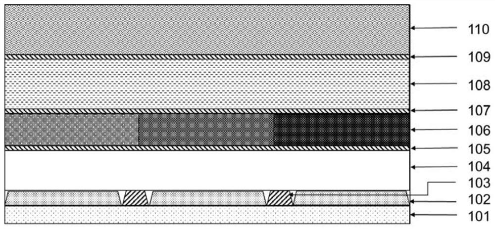
[0038] Such as Figure 1 to Figure 7 As shown, the OLED structure produced by the color silicon-based OLED preparation method of the present invention includes a CMOS substrate, an OLED layer, a first ALD film layer, a color film layer, a second ALD film layer, an encapsulation layer, and a third ALD film layer arranged in sequence. As well as the organic layer, an anode and a PDL are provided between the CMOS substrate and the OLED layer.

[0039] The preparation method of the colored silicon-based OLED of the present invention comprises the following steps:

[0040] On the CMOS substrate, the anode film is first formed by magnetron sputtering, and then the anode is formed by glue coating, exposure, development, etching, and glue removal;

[0041] Form the PDL film layer on the substrate aft...


PUM

PropertyMeasurementUnit
Thicknessaaaaaaaaaa
Thicknessaaaaaaaaaa
Thicknessaaaaaaaaaa

Abstract

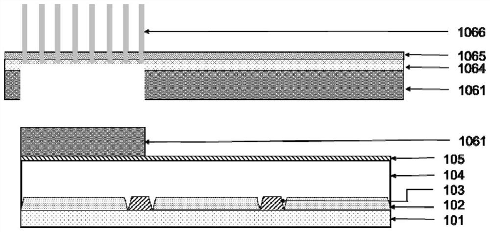
The invention discloses a preparation method of a color silicon-based OLED, which comprises the following steps of: directly transferring CF to the upper part of a first ALD layer in a vacuum environment in a laser heat transfer printing manner, and reducing the distance between the CF and an OLED light-emitting layer; meanwhile, the CF has no strong sensitivity to the temperature, so that the condition of denaturation cannot occur in the reheat transfer printing process; and by using the method to manufacture the CF, the optical crosstalk can be greatly weakened, the color gamut is improved, the visual angle is better, the process steps of water and oxygen in the product manufacturing process are reduced, and the yield loss in the product manufacturing process is reduced.

Description

technical field [0001] The invention relates to the technical field of OLED preparation, in particular to a method for preparing a colored silicon-based OLED. Background technique [0002] Organic light-emitting diode (OLED) display is recognized by the industry as the third-generation display technology after liquid crystal display (LCD) due to its thinness, active light emission, fast response speed, and rich colors. Silicon-based OLED is a subdivision of OLED. The difference from flat-panel display OLED is that silicon-based OLED is a CMOS-driven organic light-emitting device. The semiconductor 200nm process technology can be compatible with the CMOS-driven production of silicon-based OLED. Silicon-based OLED is relatively For flat panel display OLED has the following advantages, such as PPI up to 2000 or more, extremely fast response, lower power consumption, and higher integration. [0003] Due to its higher PPI, silicon-based OLEDs are mainly divided into two types of...

Claims


Application Information

Patent Timeline
IPC IPC(8): H01L51/56
CPCH10K71/00
Inventor 朱平赵铮涛刘胜芳任清江
Owner ANHUI SEMICON INTEGRATED DISPLAY TECH CO LTD
Learn More