
Buck conversion circuit and lossless absorption circuit thereof

A conversion circuit, lossless absorption technology, applied in the direction of converting DC power input to DC power output, electrical components, adjusting electrical variables, etc., can solve the problems of increasing IGBT, diode loss, temperature rise, poor characteristics, etc. Density, switching loss reduction, loss reduction effect

Pending Publication Date: 2021-06-08
苏州海鹏科技有限公司
View PDF5 Cites 1 Cited by
  • Summary
  • Abstract
  • Description
  • Claims
  • Application Information

AI Technical Summary

Problems solved by technology

[0002] The large reverse recovery current of the main diode of the BUCK circuit (that is, the step-down conversion circuit) causes a large loss and a high temperature rise of the diode, thereby limiting the increase in the power of the entire BUCK circuit, and increasing the IGBT (InsulatedGate Bipolar Transistor , insulated gate bipolar transistor) loss, EMC (ie, electromagnetic compatibility) characteristics are worse, and the energy absorbed by the buffer capacitor will eventually be consumed by resistors or equivalent passive devices

Method used


Image

  • Buck conversion circuit and lossless absorption circuit thereof

Examples


Embodiment Construction

[0011] In order to make the above objects, features and advantages of the present invention more comprehensible, the present invention will be further described in detail below in conjunction with the accompanying drawings and specific embodiments.

[0012] The term "one embodiment" or "embodiment" here refers to that specific features, structures or characteristics related to the embodiment can be included in at least one implementation of the present invention. The appearances of "in one embodiment" in various places in this specification do not necessarily all refer to the same embodiment, nor do they necessarily refer to a separate or selected embodiment that is mutually exclusive of other embodiments. "Multiple" and "several" in the present invention mean two or more. "And / or" in the present invention means "and" or "or".

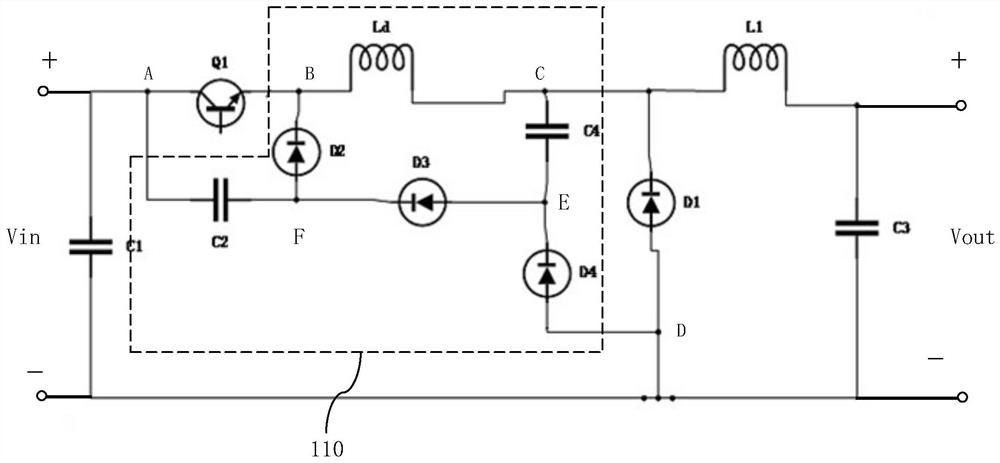
[0013] Please refer to figure 1 As shown, it is a schematic circuit diagram of a step-down conversion circuit (buck circuit) in an embodiment of the...


PUM


Abstract

The invention discloses a buck conversion circuit and a lossless absorption circuit thereof. The lossless absorption circuit comprises a first node A, a second node B, a third node C, a fourth node D, a capacitor C2, a capacitor C4, a diode D2, a diode D3, a diode D4 and an inductor Ld. One end of the capacitor C2 is connected with the first node A, the other end of the capacitor C2 is connected with the anode of the diode D2, and the cathode of the diode D2 is connected with the second node B; the inductor Ld is connected between the second node B and the third node C; one end of the capacitor C4 is connected with the third node C, the other end of the capacitor C4 is connected with the cathode of the diode D4, and the anode of the diode D4 is connected with the fourth node D; the anode of the diode D3 is connected with a connection node E between the capacitor C4 and the diode D4, and the cathode of the diode D3 is connected with a connection node F between the capacitor C2 and the diode D2. Compared with the prior art, the reverse recovery current of the main diode can be effectively improved, the turn-off loss can be reduced, the switching loss of the IGBT can be reduced, and more importantly, the temperature rise of the main diode can be reduced, and the power density of the BUCK circuit can be improved.

Description

【Technical field】 [0001] The invention relates to the technical field of switching power supplies, in particular to a step-down conversion circuit and a lossless absorption circuit thereof. 【Background technique】 [0002] The large reverse recovery current of the main diode of the BUCK circuit (that is, the step-down conversion circuit) causes a large loss and a high temperature rise of the diode, which limits the increase in the power of the entire BUCK circuit, and increases the IGBT (InsulatedGate Bipolar Transistor , insulated gate bipolar transistor) loss, EMC (ie, electromagnetic compatibility) characteristics are worse, and the energy absorbed by the buffer capacitor will eventually be consumed by resistors or equivalent passive devices. [0003] Therefore, it is necessary to provide a new technical solution to overcome the above problems. 【Content of invention】 [0004] The technical problem to be solved by the present invention is to provide a step-down conversio...

Claims


Application Information

Patent Timeline
IPC IPC(8): H02M3/155
CPCH02M3/155
Inventor 涂鹏飞
Owner 苏州海鹏科技有限公司
Learn More