Surface-treated copper foil, carrier-attached copper foil, copper-clad laminate, and printed wiring board

A printed circuit board, surface treatment technology, applied in the direction of printed circuit, printed circuit manufacturing, printed circuit components, etc., can solve the problems of circuit peeling, circuit and insulation layer adhesion reduction, etc.

Pending Publication Date: 2021-06-15
MITSUI MINING & SMELTING CO LTD
View PDF0 Cites 1 Cited by
  • Summary
  • Abstract
  • Description
  • Claims
  • Application Information

AI Technical Summary

Problems solved by technology

When this sinking occurs, the adhesive force between the circuit and the insulating layer decreases, causing the circuit to peel off

Method used


Image

  • Surface-treated copper foil, carrier-attached copper foil, copper-clad laminate, and printed wiring board
  • Surface-treated copper foil, carrier-attached copper foil, copper-clad laminate, and printed wiring board
  • Surface-treated copper foil, carrier-attached copper foil, copper-clad laminate, and printed wiring board

Examples


Embodiment

[0079] The present invention is further specifically described by the following examples.

example 1~6

[0081] Preparation and evaluation of the copper foil with a carrier and the resin replica sample were performed as follows.

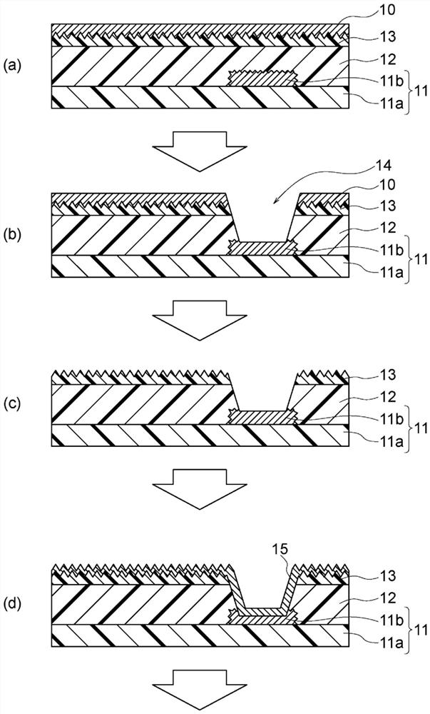
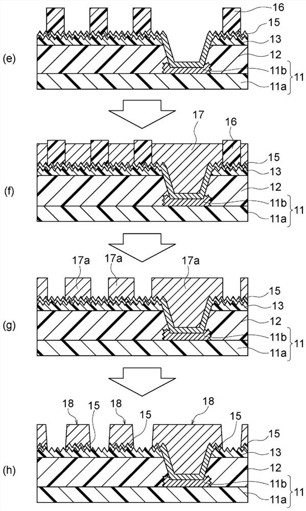
[0082] (1) Production of carrier

[0083] As a cathode, a titanium electrode whose surface was ground with a #2000 buff was prepared. In addition, DSA (dimensionally stable anode) was prepared as an anode. Using these electrodes, immersed in a copper sulfate solution with a copper concentration of 80g / L and a sulfuric acid concentration of 260g / L, at a solution temperature of 45°C and a current density of 55A / dm 2 Electrolysis was carried out to obtain an electrolytic copper foil having a thickness of 18 μm as a carrier.

[0084] (2) Formation of peeling layer

[0085] In a CBTA aqueous solution having a CBTA (carboxybenzotriazole) concentration of 1 g / L, a sulfuric acid concentration of 150 g / L, and a copper concentration of 10 g / L, the electrode surface side of the acid-washed carrier was immersed for 30 seconds at a liquid temperature of 30° C. T...


PUM

PropertyMeasurementUnit
thicknessaaaaaaaaaa
thicknessaaaaaaaaaa
thicknessaaaaaaaaaa

Abstract

Provided is a surface-treated copper foil that, in the case of use in the SAP method, can provide a resin substrate with a surface profile that can effectively prevent the generation of deposition that can be produced in a circuit in the step of etching an electroless copper plating layer. The surface-treated copper foil is a surface-treated copper foil that has a treated surface on at least one side thereof. When a resin film is hot-press bonded to the treated surface, the surface shape of the treated surface is transferred to the surface of the resin film, and the surface-treated copper film is then removed by etching, the skewness Ssk for the surface of the remaining resin film, as measured in accordance with ISO 25178, is less than or equal to -0.6.

Description

technical field [0001] The invention relates to a surface-treated copper foil, a copper foil with a carrier, a copper-clad laminate and a printed circuit board. Background technique [0002] In recent years, the semi-additive method (SAP method) has been widely used as a method of manufacturing printed wiring boards suitable for miniaturization of circuits. The SAP method is a method suitable for forming an extremely fine circuit, and as an example, it is performed using a roughened copper foil with a carrier. For example, if figure 1 and figure 2 As shown, an ultra-thin copper foil 10 having a roughened surface is pressed onto an insulating resin substrate 11 provided with a lower layer on a base substrate 11a using a prepreg 12 and an undercoat layer 13 to make it tightly bonded. In the circuit 11b (step (a)), after the carrier (not shown) is peeled off, via holes 14 are formed by laser drilling if necessary (step (b)). Then, the ultra-thin copper foil is removed by e...

Claims


Application Information

Patent Timeline
Patent Type & Authority Applications(China)
IPC IPC(8): C25D5/16C25D1/04C25D5/10C25D7/00C25D7/06H05K3/18H05K3/38
CPCC25D1/04C25D5/10C25D7/06H05K3/18H05K3/38C25D5/605H05K3/108H05K3/06H05K1/09H05K3/025C25D5/16C25D7/0614
Inventor 加藤翼松田光由
Owner MITSUI MINING & SMELTING CO LTD
Why Eureka
Try Eureka