Check patentability & draft patents in minutes with Patsnap Eureka AI!

Adapter plate and preparation method thereof

An adapter board and electrical connection technology, which is applied in semiconductor/solid-state device manufacturing, semiconductor/solid-state device components, semiconductor devices, etc., can solve the problems of inability to reduce the number of layers, delamination of wiring layers, and challenging wiring. Achieve the effect of facilitating circuit connection, reducing production time, and reducing process difficulty

Active Publication Date: 2021-11-23
浙江集迈科微电子有限公司
View PDF4 Cites 0 Cited by
  • Summary
  • Abstract
  • Description
  • Claims
  • Application Information

AI Technical Summary

Problems solved by technology

However, this setting is a great challenge for the wiring of the subsequent packaging substrate, especially for the silicon-based packaging interposer. For example, in the process of 3D packaging, most companies are trying to minimize the surface of the silicon-based interposer Number of wiring layers to reduce warping of the silicon-based interposer due to too many wiring layers in the silicon
Although the number of wiring layers can be reduced by increasing the wiring density, in the special wiring settings of RF wiring, considering the problems of crosstalk and insertion loss between inter-layer signals, it is often impossible for the module to increase the wiring density of certain layers. reduce the number of layers
Therefore, the multi-layer wiring with a large thickness in the RF chip is a big challenge for the production process of the large-sized and thin interposer board and the subsequent micro-assembly process. At the same time, too many wiring layers are easy Delamination of wiring layers due to high stress occurs

Method used


Image

  • Adapter plate and preparation method thereof
  • Adapter plate and preparation method thereof
  • Adapter plate and preparation method thereof

Examples


Embodiment 1

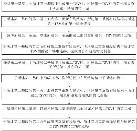
[0070] refer to Figure 2~Figure 12 , this embodiment provides an adapter board, the adapter board includes:

[0071] Composite wiring structure 100, said composite wiring structure 100 includes:

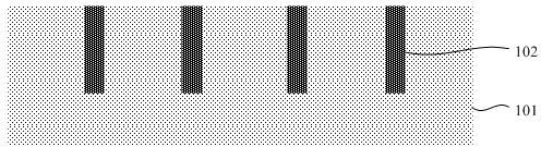
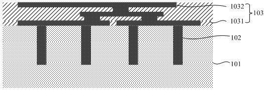
[0072] A first base 101, wherein the first base 101 has a first TSV column 102, and the first TSV column 102 runs through the first base 101;

[0073] A first rewiring structure 103, the first rewiring structure 103 is located on the first surface of the first substrate 101, and is electrically connected to the first end of the first TSV column 102;

[0074] A second rewiring structure 104, the second rewiring structure 104 is located on the second surface of the first substrate 101, and is electrically connected to the second end of the first TSV column 102;

[0075] The adapter board also includes:

[0076] The second substrate 201, the second substrate 201 has a second TSV column 202 and a groove 203, the second TSV column 202 penetrates the second substrate 201, and the compo...

Embodiment 2

[0115] refer to Figure 14~Figure 19 , this embodiment also provides an adapter board, the difference between the adapter board and the adapter board in Embodiment 1 is that the second base 301 further includes a third TSV column 303, wherein the groove 305 exposes the first end of the third TSV column 303, the second surface of the second substrate 301 exposes the second end of the third TSV column 303, and the third TSV column 303 is respectively combined with the The wiring structure 100 and the fourth rewiring structure 304 are electrically connected, so that in this embodiment, compared with the first embodiment, the double-sided electrical extraction of the composite wiring structure 100 can be further realized through the third TSV column 303 , so that the transmission path can be reduced, the transmission efficiency can be improved, and the loss can be reduced.

[0116] For the structure of the adapter plate, please refer to Embodiment 1, which will not be introduced ...


PUM


Abstract

The present invention provides an adapter board and a preparation method thereof. Firstly, a composite wiring structure having a first substrate, a first rewiring structure and a second rewiring structure is prepared, and then the composite wiring structure with a certain metal wiring layer is placed in the In the groove of the second substrate with TSV pillars, the composite wiring structure is electrically connected to the rewiring structure on the surface of the second substrate, thereby finally forming an interposer board with densely wired areas and sparsely wired areas, which can solve the problem of Quality problems such as warping and delamination caused by the high stress caused by multi-layer wiring can also reduce the production time of the adapter board, reduce the difficulty of the process, and facilitate subsequent circuit connections.

Description

technical field [0001] The invention relates to the technical field of semiconductors, in particular to an adapter board and a preparation method thereof. Background technique [0002] Millimeter wave radio frequency technology is developing rapidly in the semiconductor industry, and it has been widely used in high-speed data communications, automotive radar, airborne missile tracking systems, and spatial spectral detection and imaging. New applications have put forward new requirements for the electrical performance, compact structure and system reliability of the product. For wireless transmitting and receiving systems, they cannot be integrated into the same chip (SOC), so it is necessary to integrate different chips such as radio frequency units, filters, power amplifiers, etc. into an independent system to achieve The function of transmitting and receiving signals. [0003] For most radio frequency chips, because the transmission of radio frequency signals needs to cr...

Claims


Application Information

Patent Timeline
Patent Type & Authority Patents(China)
IPC IPC(8): H01L23/498H01L21/48
CPCH01L21/4846H01L21/485H01L21/4857H01L21/486H01L23/49805H01L23/49822H01L23/49827H01L23/49838
Inventor 冯光建郭西黄雷高群
Owner 浙江集迈科微电子有限公司
Features
  • R&D
  • Intellectual Property
  • Life Sciences
  • Materials
  • Tech Scout
  • Unparalleled Data Quality
  • Higher Quality Content
  • 60% Fewer Hallucinations
Learn More