Vanadium dioxide metamaterial structure capable of realizing tunable ultra wide band and application of vanadium dioxide metamaterial structure
A vanadium dioxide and metamaterial technology, applied in refrigeration and liquefaction, electrical components, refrigerators, etc., can solve the problems of difficult vanadium dioxide structure processing, low material refrigeration power, weak absorption effect, etc., to achieve simple graphics, The effect of high cooling power and enhanced absorption rate
- Summary
- Abstract
- Description
- Claims
- Application Information
AI Technical Summary
Problems solved by technology
Method used
Image
Examples
Embodiment 1
[0042] A vanadium dioxide metamaterial for tunable ultra-broadband, such as Figure 1-3 As shown, including a multi-layer substrate, a patterned vanadium dioxide layer 2 and a top random particle layer 1:
[0043] The base layer includes a silicon dioxide layer 3, a silicon nitride layer 4, and a metal silver layer 5 arranged from top to bottom, and their thicknesses are respectively t 3 =0.1 μm, t 4 =0.5 μm, t 5 =0.2μm;
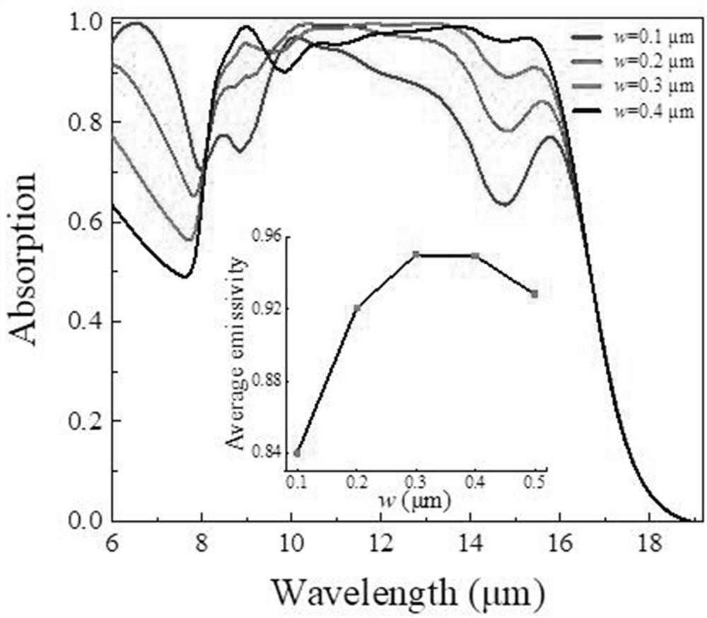
[0044] The pattern of the patterned vanadium dioxide layer 2 is a continuum array formed by the arrangement of structural units without gaps. The structural units are squares, and L-shaped vanadium dioxide is arranged at the four corners of the square. In the center of the square Correspondingly, a cylinder of vanadium dioxide is provided, and the lengths of the two right-angled sides of the L-type vanadium dioxide are equal, and there is a certain distance between adjacent L-type vanadium dioxide; when the vanadium dioxide is in a metal phase, the metama...
Embodiment 2
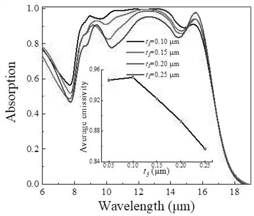
[0047] The difference between this embodiment and Embodiment 1 is that, keeping other conditions unchanged, the thickness of the silicon dioxide layer is adjusted to be t 3 =0.1 μm, t 3 =0.15μm,t 3 =0.20μm,t 3 =0.25μm, and measure the emissivity of the material, the result is as Figure 4 shown. Depend on Figure 4 It can be obtained that the thickness of the silicon dioxide layer is t 3 =0.1 μm, the emissivity is higher in the range of 8-16 μm.
Embodiment 3
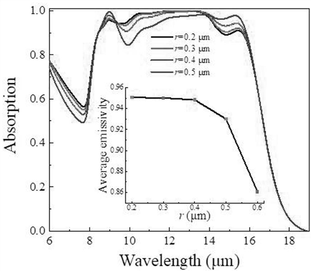
[0049] The difference between this example and Example 1 is that, keeping other conditions unchanged, the radii of the vanadium dioxide cylinders are adjusted to r=0.2 μm, r=0.3 μm, r=0.4 μm, r=0.5 μm , and measure the emissivity of the material, the result is as Figure 5 shown. Depend on Figure 5 It can be obtained that when the vanadium dioxide cylinder radius r=0.3 μm, the emissivity in the range of 8-16 μm is higher.
PUM
| Property | Measurement | Unit |
|---|---|---|
| thickness | aaaaa | aaaaa |
| length | aaaaa | aaaaa |
| width | aaaaa | aaaaa |
Abstract
Description
Claims
Application Information


