
Interferometer device and method for producing an interferometer device

An interferometer, area technology, applied in interferometers, measuring devices, using optical devices, etc., can solve problems such as damage to optical quality

Pending Publication Date: 2021-06-25
ROBERT BOSCH GMBH
View PDF7 Cites 0 Cited by
  • Summary
  • Abstract
  • Description
  • Claims
  • Application Information

AI Technical Summary

Problems solved by technology

However, this may have a charging effect of the pn junction (voltage-dependent parasitic capacitance) and cause leakage currents
Furthermore, this optical region must also be at least weakly doped, which can impair the optical quality of these layers

Method used


Image

  • Interferometer device and method for producing an interferometer device
  • Interferometer device and method for producing an interferometer device
  • Interferometer device and method for producing an interferometer device

Examples


Embodiment Construction

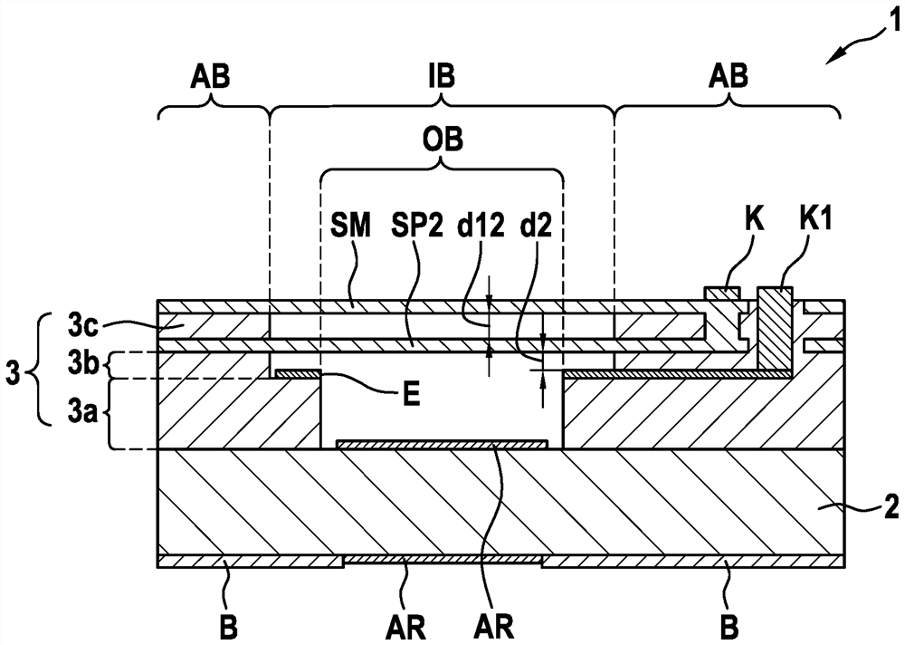
[0049] figure 1 A schematic side cross-sectional view of an interferometer device according to an embodiment of the invention is shown.

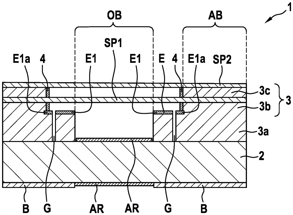
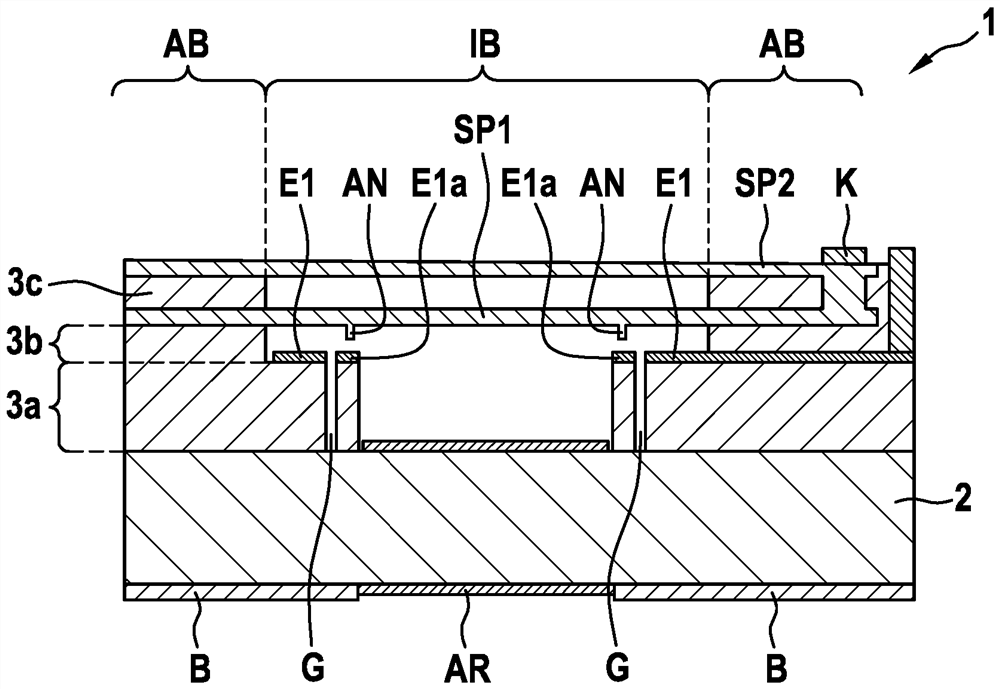
[0050] The interferometer arrangement 1 comprises: a substrate 2; an intermediate layer region 3 applied on the substrate 2; a first mirror arrangement SP1 and a second mirror arrangement SP2, wherein the first mirror arrangement and the second mirror arrangement are opposite are aligned plane-parallel to each other and are spaced apart from each other by a first distance d12 and are enclosed in or arranged on the intermediate layer region 3 , wherein the intermediate layer region 3 is in the inner region IB of the first mirror arrangement SP1 are removed below and below the second mirror arrangement SP2; and a laterally structured electrode E, wherein the laterally structured electrode comprises a first subregion E1 and at least one laterally separated from the first subregion and an electrically insulating second sub-region (not shown), w...


PUM


Abstract

The invention relates to an interferometer device (1), comprising: a substrate (2); an intermediate layer region (3), which is applied to the substrate (2); a first mirror device (SP1) and a second mirror device (SP2), which are oriented plane-parallel to one another, are spaced apart from one another by a first distance (d12) and are enclosed in or arranged on the intermediate layer region (3), the intermediate layer region (3) being removed below the first mirror device (SP1) and / or below the second mirror device (SP2) in an inner region (IB); and a laterally structured electrode (E), which comprises a first subregion (E1) and at least one second subregion (E2), which is laterally separated from and electrically insulated from the first subregion, which subregions can be connected to different electric potentials, wherein: the electrode (E) is spaced apart from the first or the second mirror device (SP1; SP2) by a second distance (d2); the first subregion (E1) runs in the inner region (IB) and is arranged on the intermediate layer region (3) and the second subregion (E2) runs in an outer region (AB) of the intermediate layer region (3), such that the first mirror device (SP1) and / or the second mirror device (SP2) can be moved electrostatically in the inner region (IB) by means of the first subregion (E1), parallel to the substrate (2), and the first distance (d12) can be varied.

Description

technical field [0001] The invention relates to an interferometer device and a method for producing the interferometer device. Background technique [0002] To miniaturize tunable spectral filters, Fabry-Pérot interferometers (FPIs) can advantageously be implemented in MEMS technology. The advantage here is that a cavity consisting of two plane-parallel, highly reflective mirrors with a distance (cavity length) exhibits strong transmission in the optical wavelength range only for wavelengths in which The lower cavity length corresponds to an integer multiple of half a wavelength. The cavity length can be varied, for example, by means of electrostatic or piezoelectric actuation, resulting in a spectrally tunable filter element. Most of the known FPIs use (in contrast to the piezoelectric drive mentioned above) the electrostatic drive of mirrors, which are often designed as membranes. In this case, a voltage is applied between two electrodes, which lie in the plane of the t...

Claims


Application Information

Patent Timeline
Patent Type & Authority Applications(China)
IPC IPC(8): G01J3/26G01J3/02G01J3/32G01J3/453
CPCG01J3/0256G01J3/4532G01J3/26G01J3/32G01J3/4535G02B5/288G02B26/007G02B26/06G01B9/02G01B2290/25
Inventor B·斯泰因M·胡思尼克C·谢林T·布克C·D·克莱默R·勒德尔
Owner ROBERT BOSCH GMBH
Learn More