
Crimping type power semiconductor module structure and subunit and manufacturing method thereof

A technology of power semiconductor and module structure, which is applied in the direction of semiconductor devices, electrical components, electric solid devices, etc., can solve the problems of being easily disturbed and restricted by the environment, unable to monitor the chip junction temperature, and the limitations of junction temperature monitoring, etc., to achieve the realization of Effects of long-distance signal transmission, light weight, and small structural influence

Pending Publication Date: 2021-07-02
CHONGQING UNIV
View PDF9 Cites 0 Cited by
  • Summary
  • Abstract
  • Description
  • Claims
  • Application Information

AI Technical Summary

Problems solved by technology

[0005] In view of this, the object of the present invention is to provide a crimping type power semiconductor module structure with real-time temperature monitoring function and its subunit and manufacturing method, to solve the limitations of junction temperature monitoring of traditional crimping type power semiconductor devices, It is impossible to monitor the junction temperature of all chips, and it is easy to be disturbed and restricted by the environment

Method used


Image

  • Crimping type power semiconductor module structure and subunit and manufacturing method thereof
  • Crimping type power semiconductor module structure and subunit and manufacturing method thereof
  • Crimping type power semiconductor module structure and subunit and manufacturing method thereof

Examples


Embodiment Construction

[0031] Embodiments of the present invention are described below through specific examples, and those skilled in the art can easily understand other advantages and effects of the present invention from the content disclosed in this specification. The present invention can also be implemented or applied through other different specific implementation modes, and various modifications or changes can be made to the details in this specification based on different viewpoints and applications without departing from the spirit of the present invention. It should be noted that the diagrams provided in the following embodiments are only schematically illustrating the basic concept of the present invention, and the following embodiments and the features in the embodiments can be combined with each other in the case of no conflict.

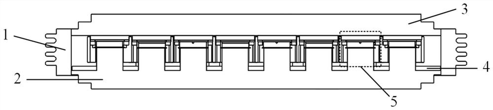
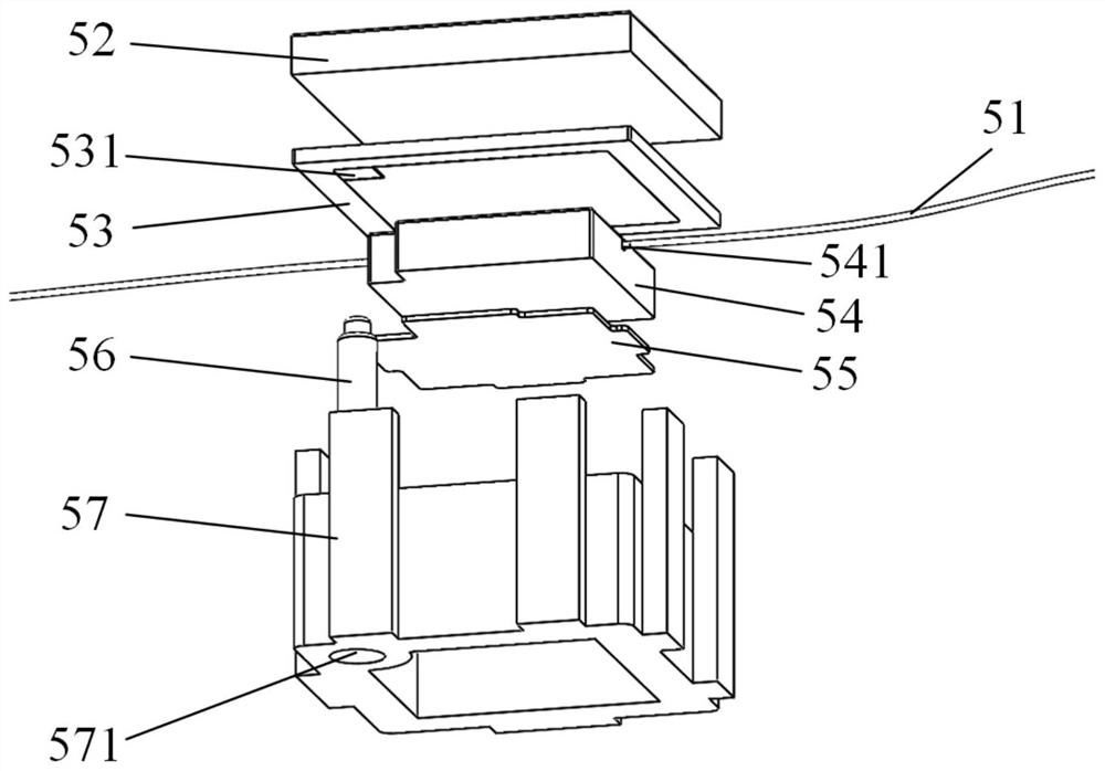
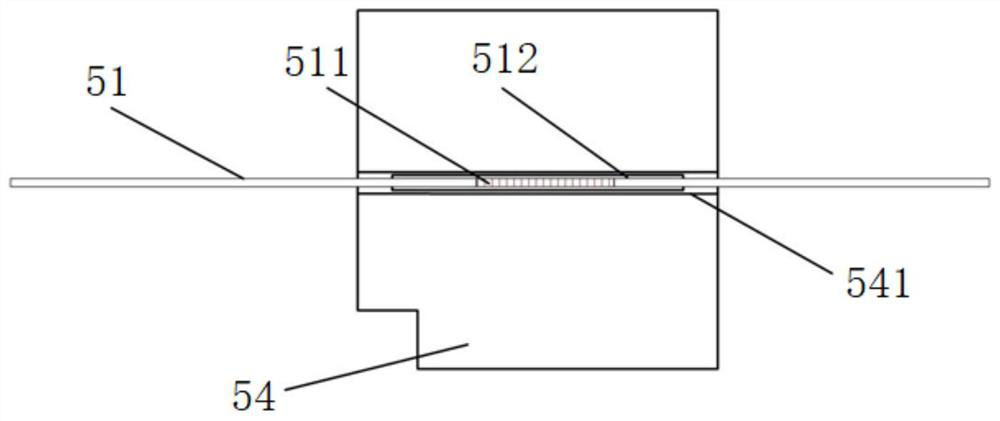
[0032] Wherein, the accompanying drawings are for illustrative purposes only, and represent only schematic diagrams, rather than physical drawings, and should...


PUM

PropertyMeasurementUnit
thicknessaaaaaaaaaa

Abstract

The invention relates to a crimping type power semiconductor module structure and a subunit and a manufacturing method thereof, and belongs to the field of power semiconductor devices. The structure comprises an insulating frame, and a silver sheet, a lower molybdenum sheet, a chip and an upper molybdenum sheet which are sequentially stacked in the insulating frame from bottom to top; the insulating frame is provided with a spring needle, and the spring needle is connected with the grid electrode of the chip; the surface, in contact with the chip, of the lower molybdenum sheet is provided with a horizontally-through groove, the optical fiber penetrates through the groove, and more than one grating is integrated on the optical fiber in the groove. The distributed online real-time measurement of the junction temperature of the chip in the device package can be conveniently realized. Moreover, the fiber grating is small in size, light in weight, small in influence on the structure and easy to arrange; and only the installation step of the fiber bragg grating needs to be added in the normal packaging process. The electrical insulating property of the optical fiber manufacturing material is good, and the structure and the function of the crimping type power semiconductor module are not affected after integration.

Description

technical field [0001] The invention belongs to the field of power semiconductor devices, and relates to a crimping type power semiconductor module structure, subunits and a manufacturing method thereof. Background technique [0002] Large-capacity crimp-type IGBT devices are packaged in parallel with multiple chips, and the junction temperature distribution of parallel chips is often uneven. The simulation results show that during the working process of the device, due to the thermal deformation of the packaging structure, the junction temperature of different chips can vary by tens of degrees Celsius at most. In order to avoid device failure caused by local chip overheating and improve the operating reliability of the converter, it is necessary to monitor the operating junction temperature distribution of the press-connected IGBT device online. [0003] The junction temperature monitoring methods of power devices can be divided into direct measurement method and indirect ...

Claims


Application Information

Patent Timeline
Patent Type & Authority Applications(China)
IPC IPC(8): H01L25/07H01L25/18H05K1/18H05K3/32G01K11/32
CPCH01L25/072H01L25/18H05K1/181H05K3/325G01K11/32
Inventor 任海冉立蒋华平刘立王小勇
Owner CHONGQING UNIV
Features
  • Generate Ideas
  • Intellectual Property
  • Life Sciences
  • Materials
  • Tech Scout
  • Unparalleled Data Quality
  • Higher Quality Content
  • 60% Fewer Hallucinations
Learn More