Semiconductor structure, self-annealing chip and manufacturing method of semiconductor structure

A semiconductor and protection structure technology, applied in the fields of semiconductor/solid-state device manufacturing, semiconductor devices, semiconductor/solid-state device components, etc. Problems such as limited layout area and poor versatility to ensure real-time and accuracy, high versatility, and enhanced versatility

Pending Publication Date: 2021-07-30
北京锐达芯集成电路设计有限责任公司
View PDF0 Cites 0 Cited by
  • Summary
  • Abstract
  • Description
  • Claims
  • Application Information

AI Technical Summary

Problems solved by technology

This scheme has a high degree of integration, but it mainly performs annealing treatment by applying an external control source, and its annealing effect is more dependent on the external control program. When the external radiation environment changes irregularly, it cannot guarantee the real-time annealing treatment. reliability, accuracy and reliability, when a total dose radiation effect leakage occurs, it is easy to cause the collapse of the entire system
At the same time, the heater or heating element integrated in the semiconductor substrate has limited layout area and poor versatility

Method used


Image

  • Semiconductor structure, self-annealing chip and manufacturing method of semiconductor structure
  • Semiconductor structure, self-annealing chip and manufacturing method of semiconductor structure
  • Semiconductor structure, self-annealing chip and manufacturing method of semiconductor structure

Examples


Embodiment Construction

[0040] In order to facilitate the understanding of the present invention, the present invention will be described more fully below with reference to the associated drawings. Preferred embodiments of the invention are shown in the accompanying drawings. However, the present invention can be implemented in different forms and is not limited to the embodiments described herein. On the contrary, these embodiments are provided to make the understanding of the disclosure of the present invention more thorough and comprehensive.

[0041] Below, the technical solution of the present invention will be described in detail with reference to the accompanying drawings.

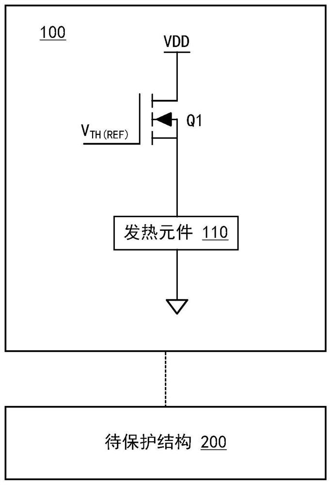
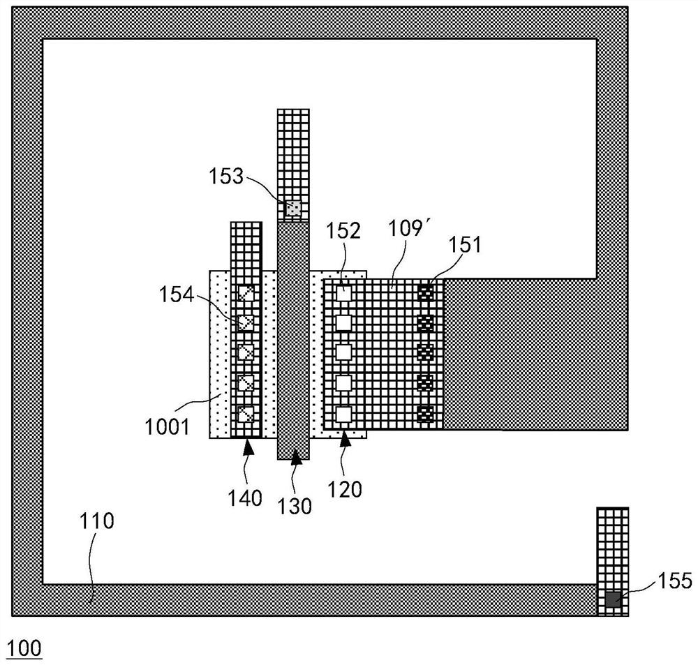
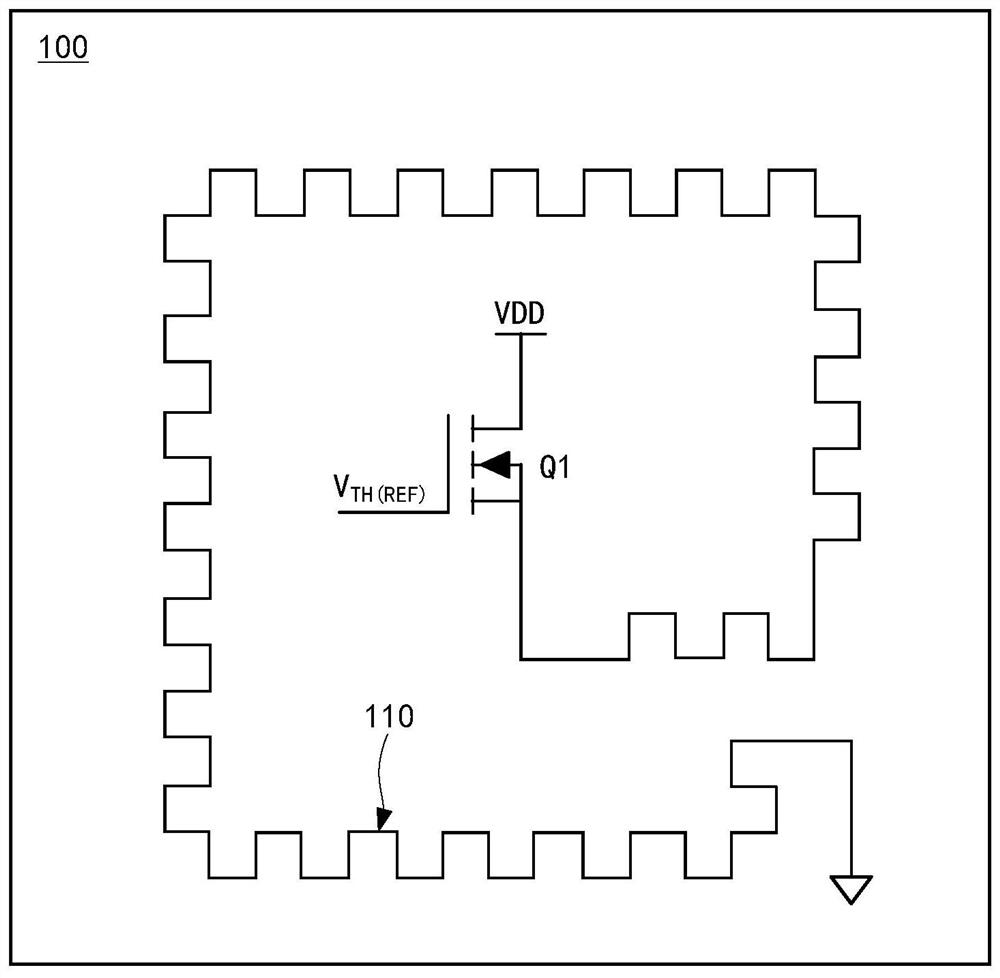
[0042] Such as figure 1 As shown, in the present disclosure, the self-annealing chip includes a semiconductor structure 100 and a structure to be protected 200 , and the semiconductor structure 100 can be thermally annealed to the structure to be protected 200 . Wherein, the semiconductor structure 100 and the structure...


PUM


Abstract

The invention discloses a semiconductor structure, a self-annealing chip and a manufacturing method of the semiconductor structure. The semiconductor structure comprises an N-type MOSFET and a heating element which are connected in series between an excitation signal input end and a reference ground, wherein the grid electrode of the N-type MOSFET receives a bias voltage; when the N-type MOSFET is subjected to external radiation, the threshold voltage is reduced, and under the condition that the threshold voltage is reduced to be smaller than or equal to the bias voltage, the N-type MOSFET is conducted so as to control the heating element to heat; in the heating process, self-annealing is recovered, and under the condition that the self-annealing is recovered to be greater than the bias voltage, the heating element is controlled to stop heating; the heating element is located in the dielectric layer of the upper layer surface of the N-type MOSFET and is connected with the source electrode of the N-type MOSFET through the wiring layer. The settable area of the heating element in the semiconductor structure is not limited, the arrangement is flexible, meanwhile, the semiconductor structure can automatically start / close the thermal annealing treatment function according to the drifting condition of the threshold voltage of the N-type MOSFET, and the real-time performance and accuracy of thermal annealing treatment are effectively guaranteed.

Description

technical field [0001] The invention relates to the technical field of semiconductors, in particular to a semiconductor structure, a self-annealing chip and a method for manufacturing the semiconductor structure. Background technique [0002] For equipment that has been working in an external radiation environment for a long time, the semiconductor devices in it will have problems such as threshold voltage drift, transconductance decrease, sub-threshold current increase, and low-frequency noise increase under the action of continuous ionizing radiation, which may even cause The device fails, which is the total dose radiation effect. The total dose irradiation effect is mainly caused by the charges and defects generated by ionizing radiation in the oxide layer and the oxide layer or silicon interface. [0003] Previous studies have shown that when the irradiated semiconductor device is subjected to heat treatment, that is, annealing, the trapped holes in the oxide layer of t...

Claims


Application Information

Patent Timeline
Patent Type & Authority Applications(China)
IPC IPC(8): H01L23/34H01L29/78H01L21/336
CPCH01L23/345H01L29/66477H01L29/78
Inventor 张葳张薇邢康伟朱恒宇
Owner 北京锐达芯集成电路设计有限责任公司
Why Eureka
Try Eureka