Ceramic carrier plate for polishing semiconductor wafers

A semiconductor and wafer technology, applied in the field of ceramic carrier, can solve the problems of low temperature and unaccelerated removal rate, and achieve the effects of simple and easy processing technology, accelerated chemical reaction speed, and small deviation

Inactive Publication Date: 2021-08-06
FUJIAN JING AN OPTOELECTRONICS CO LTD
View PDF12 Cites 1 Cited by
  • Summary
  • Abstract
  • Description
  • Claims
  • Application Information

AI Technical Summary

Problems solved by technology

[0003] In view of the problems occurring in the above-mentioned semiconductor wafer processing process, the present invention provides a semiconductor wafer polishing method, which uses the ceramic carrier disc provided by the present invention for semiconductor wafer polishing in the polishing process to solve the problem of semiconductor wafer polishing. During the polishing process, the removal rate cannot be accelerated due to low temperature, and at the same time, it ensures that the wafer will not slip and shake during processing, and the processing quality of the wafer is guaranteed.

Method used


Image

  • Ceramic carrier plate for polishing semiconductor wafers
  • Ceramic carrier plate for polishing semiconductor wafers

Examples


Embodiment Construction

[0029] In order to make the purpose, technical solutions and advantages of the embodiments of the present invention more clear, the embodiments of the present invention will be further described in detail below in conjunction with the accompanying drawings. Here, the exemplary embodiments and descriptions of the present invention are used to explain the present invention, but not to limit the present invention.

[0030] It should be noted in advance that the term "comprising / comprising" used herein refers to the presence of features, elements, steps or components, but does not exclude the existence of one or more other features, elements, steps or components.

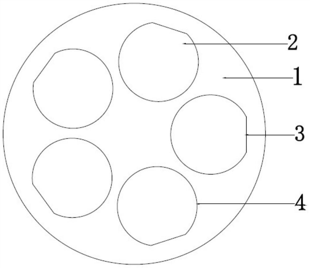
[0031] as attached figure 1 Shown is a top view of the ceramic carrier plate in an embodiment of the present invention, its structure includes: a plate body 1, a groove 2 located on the plate body, the groove and the plate body are integrated, and the top of the groove is flush with the plate body , and the grooves are...


PUM

PropertyMeasurementUnit
surface smoothnessaaaaaaaaaa
softening pointaaaaaaaaaa
thicknessaaaaaaaaaa

Abstract

The invention discloses an integral polishing ceramic carrier plate for wax-free polishing of semiconductor wafers. The ceramic carrier plate comprises a plate body and a groove located on the plate body, the groove and the plate body are integrated, the top of the groove is flush with the plate body, the groove is distributed on the periphery of the upper end of the plate body and is in a rotational symmetry shape, and the groove is used for bearing the semiconductor wafers. The problems that the temperature is low in the polishing process of the semiconductor wafers and the removal rate cannot be increased are solved, meanwhile, it is guaranteed that the wafers cannot slide and shake in the machining process, and the machining quality of the wafers is guaranteed.

Description

technical field [0001] The invention relates to the technical field of crystal growth processing, in particular to a ceramic carrier used for semiconductor wafer polishing. Background technique [0002] In order to ensure that the TTV (Total Thickness Variation, substrate thickness difference) and surface roughness after semiconductor wafer processing are in compliance, the wafer needs to be fixed with wax before polishing. Since the softening temperature of the wax is about 40°C, the temperature of the semiconductor wafer cannot exceed 40°C when it is polished or polished, otherwise it will cause slippery wax during the polishing process, and the wafer will fall off and cause fragments. However, the higher the temperature, the chemical in the polishing process. The faster the reaction speed, the higher the temperature in the polishing process of the semiconductor wafer due to the presence of the wax, and the insufficient chemical action in the polishing process, the removal...

Claims


Application Information

Patent Timeline
Patent Type & Authority Applications(China)
IPC IPC(8): B24B37/30B24B37/10B24B7/22
CPCB24B37/30B24B37/10B24B7/228
Inventor 李瑞评曾柏翔张佳浩杨良陈铭欣
Owner FUJIAN JING AN OPTOELECTRONICS CO LTD
Why Eureka
Try Eureka