Diode chip structure and manufacturing method

A manufacturing method and diode technology, which are applied in semiconductor/solid-state device manufacturing, electrical components, circuits, etc., can solve problems such as increased loss, increased MOS tube pressure, and increased MOS tube overshoot voltage to reduce overshoot voltage. , Increase the softness, slow recovery characteristics more effect

Active Publication Date: 2021-08-13
SHENZHEN BASIC SEMICON LTD
View PDF10 Cites 0 Cited by
  • Summary
  • Abstract
  • Description
  • Claims
  • Application Information

AI Technical Summary

Problems solved by technology

The conventional flyback converter circuit is shown in Figure 1 The disadvantage of this circuit is that due to the influence of component parasitic parameters, ringing and overshoot will occur at the drain of the switch tube, resulting in increased pressure on the MOS tube and increased loss
These two methods can effectively suppress the ringing, but both will significantly increase the overshoot voltage at the moment of cut-off of the MOS tube

Method used


Image

  • Diode chip structure and manufacturing method
  • Diode chip structure and manufacturing method
  • Diode chip structure and manufacturing method

Examples


Embodiment Construction

[0071] In order to make the object, technical solution and advantages of the present invention clearer, the present invention will be further described in detail below in conjunction with the accompanying drawings and specific embodiments. It should be understood that the specific embodiments described here are only used to explain the present invention, not to limit the present invention.

[0072] The invention provides a method for manufacturing a diode chip.

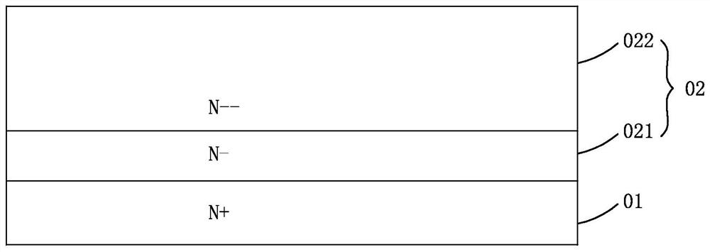
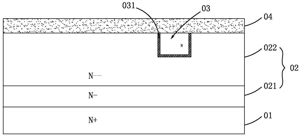
[0073] Step A, please refer to figure 2 , at least one epitaxial layer 02 of a first conductivity type is formed on the substrate 01 , and the first conductivity type is the same as that of the substrate 01 . In this implementation manner, the first conductivity type is N type. In this embodiment, the epitaxial layer 02 has two layers, including the first epitaxial layer 021 and the second epitaxial layer 022 from bottom to top, and the resistivity and thickness of the second epitaxial layer 022 are both Correspon...


PUM


Abstract

The invention discloses a diode chip manufacturing method. According to the method, at least one epitaxial layer is formed on a substrate; a groove region is formed on the epitaxial layer; ion implantation and diffusion are carried out through a first process condition, so that a first well region corresponding to the transverse PN junction is formed in the groove region, a second well region corresponding to the longitudinal PN junction is formed on the epitaxial layer, and a plurality of third well regions used for terminal ring regions are formed on the epitaxial layer; multiple times of ion implantation and diffusion are conducted under different process conditions so as to longitudinally form doped regions with different concentrations in the three well regions respectively; and a subsequent process is conducted to complete the manufacturing of the diode chip. The invention further discloses a diode chip structure. The technology is simple in process, the manufactured diode chip structure is smaller in size, the slow recovery characteristic is better, and the overshoot voltage at the cut-off moment of the MOS tube electrically connected with the diode chip structure can be greatly reduced in the flyback converter.

Description

technical field [0001] The invention relates to the technical field of semiconductor devices, in particular to a diode chip structure and a manufacturing method. Background technique [0002] Flyback converter is also called single-ended flyback converter. It gets its name because the output terminal gets energy when the primary winding is disconnected from the power supply. The flyback converter is popular among development engineers because of its simple circuit structure and low cost. A conventional flyback converter circuit such as figure 1 As shown, the disadvantage of this circuit is: due to the influence of component parasitic parameters, ringing and overshoot will occur at the drain of the switch tube, which will increase the pressure of the MOS tube and increase the loss. The ringing is caused by the oscillation circuit composed of leakage inductance Lleak, Rclp and Clump when the MOS is turned off. [0003] The traditional method of suppressing ringing is: in ...

Claims


Application Information

Patent Timeline
Patent Type & Authority Applications(China)
IPC IPC(8): H01L21/329H01L29/861H01L29/06H01L29/36
CPCH01L29/66136H01L29/861H01L29/0603H01L29/0684H01L29/36Y02P70/50
Inventor 李学会孙军温正欣和巍巍汪之涵傅俊寅魏炜
Owner SHENZHEN BASIC SEMICON LTD
Why Eureka
Try Eureka