Method for manufacturing back electrode of CdTe solar cell
A technology for a solar cell and a manufacturing method, which is applied to circuits, electrical components, photovoltaic power generation, etc., can solve the problems of waste of photoresist, lengthy and complicated laser engraving process, etc., so as to improve the precision of engraving, improve the yield rate, and simplify the process. The effect of the process
Pending Publication Date: 2021-08-17
CHINA TRIUMPH INT ENG
View PDF6 Cites 2 Cited by
- Summary
- Abstract
- Description
- Claims
- Application Information
AI Technical Summary
Problems solved by technology
[0003] In view of the above-mentioned shortcomings of the prior art, the purpose of the present invention is to provide a method for manufacturing the back electrode of a CdTe solar cell, which is used to solve the problems of lengthy and complicated laser scribing procedures and a large amount of waste of photoresist in the prior art
Method used
View moreImage
Smart ImageViewing Examples
Examples
Embodiment Construction
[0030] The embodiments of the present invention will be easily understood by those skilled in the
[0031] As described in detail the embodiments of the present invention, in order to facilitate explanation, the cross-sectional view representing the device structure is not in general ratio, and the schematic diagram is merely an example, which is not to limit the scope of the invention. In addition, the three-dimensional spatial dimensions of length, width, and depth should be included in the actual production.
[0032] For convenience of description, there may be a space relationship word such as "under", "below", "lower", "below", "above", "upper", and the like may be used to describe ...
Login to View More PUM
| Property | Measurement | Unit |
|---|---|---|
| Thickness | aaaaa | aaaaa |
| Thickness | aaaaa | aaaaa |
| Width | aaaaa | aaaaa |
Abstract
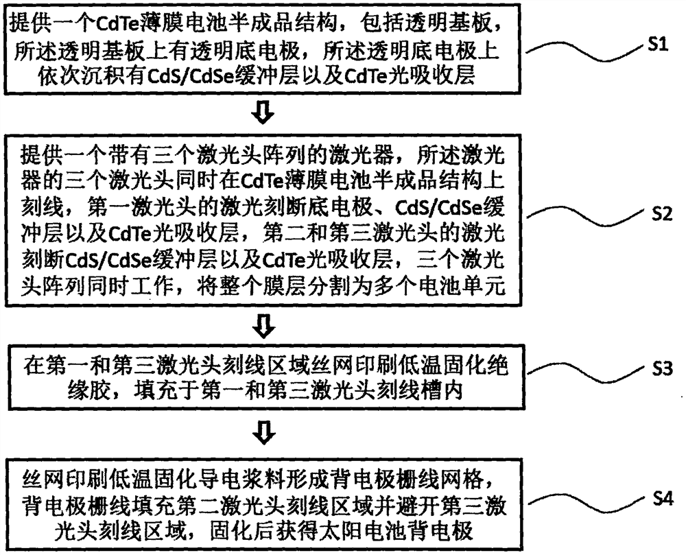
The invention provides a method for manufacturing a back electrode of a CdTe solar cell, and the method is characterized in that a laser with three laser head arrays is used for simultaneously etching lines on a CdTe light absorption layer of a CdTe thin film cell semi-finished product structure; a bottom electrode, a buffer layer and the light absorption layer are etched by the laser of a first laser head, and the buffer layer and the light absorption layer are etched by the laser of a second laser head and a third laser head; the three laser head arrays work at the same time, and the whole film layer is divided into a plurality of battery units; silk-screen printing is performed on low-temperature curing insulation paste in the first and third laser head scribing areas, and the low-temperature curing insulation paste is put in the first and third laser head scribing grooves; silk-screen printing is performed on the low-temperature curing conductive slurry to form a back electrode grid line grid, back electrode grid lines are kept away from a third laser head scribing area, and curing is performed to obtain the back electrode of the solar cell. The method simplifies the technological process, reduces the environmental protection pressure, remarkably reduces the cost in the technological process, and improves the yield.
Description
Technical field [0001] The present invention belongs to the field of photovoltaic cells, and in particular, the present invention relates to a method of making a back electrode for a CDTE solar cell. Background technique [0002] Cadmium telluride solar cells are a thin film solar cell based on the heterojunction of P-type CDTE and N-type CDS / CDSE, which is easy to make, low cost and weight, and so on. The production cost of the cadmium telluride thin film solar cell is much lower than the solar cell technology of crystalline silicon and other materials. Second it is consistent with the sun spectrum, absorbs more than 95% of the sunshine. During the size of the CDTE solar cell, the multi-layer membrane structure cutting and metallization of the metal is needed to form a multi-battery sheet series structure assembly, and the cutting is achieved by multiple laser engraved processing, and solar energy is easily occurring during processing. The non-straightness of the thin film bat...
Claims
Login to View More Application Information
Patent Timeline
 IPC IPC(8): H01L31/0224H01L31/0296
CPCH01L31/022425H01L31/0296Y02E10/50
Inventor 彭寿汪元元吴一民马立云殷新建陈瑛
Owner CHINA TRIUMPH INT ENG


