Silicon wafer batch polishing equipment

A technology for silicon wafers and equipment, which is applied in the field of batch polishing equipment for silicon wafers, can solve problems such as the inability to polish silicon wafers at the same time, and achieve the effect of improving efficiency

Inactive Publication Date: 2021-08-20
周勤
View PDF0 Cites 0 Cited by
  • Summary
  • Abstract
  • Description
  • Claims
  • Application Information

AI Technical Summary

Problems solved by technology

The invention is mainly used to solve the problem of low polishing efficiency of existing silicon wafer polishing equipment because it cannot simultaneously polish many silicon wafers at one time

Method used


Image

  • Silicon wafer batch polishing equipment
  • Silicon wafer batch polishing equipment
  • Silicon wafer batch polishing equipment

Examples


Embodiment Construction

[0038] In order to make the technical means, creative features, goals and effects achieved by the present invention easy to understand, the present invention will be further described below in conjunction with specific embodiments.

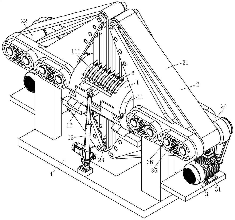
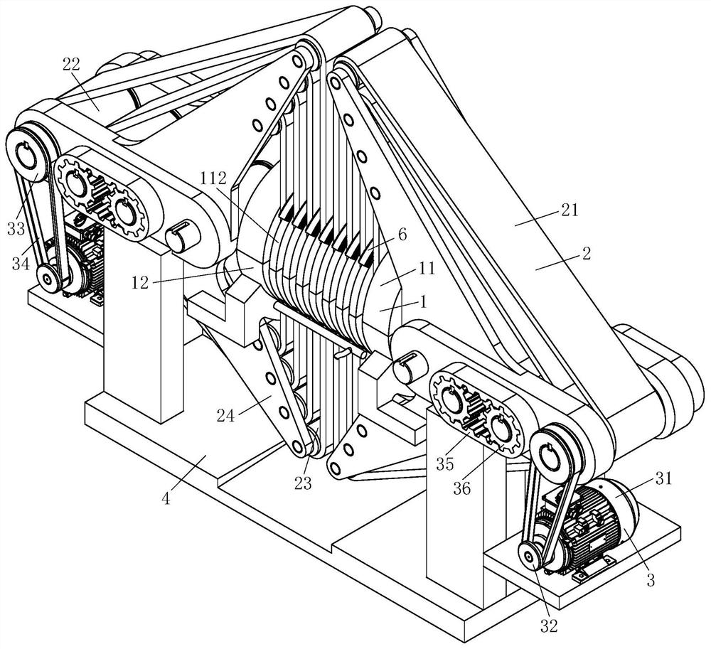
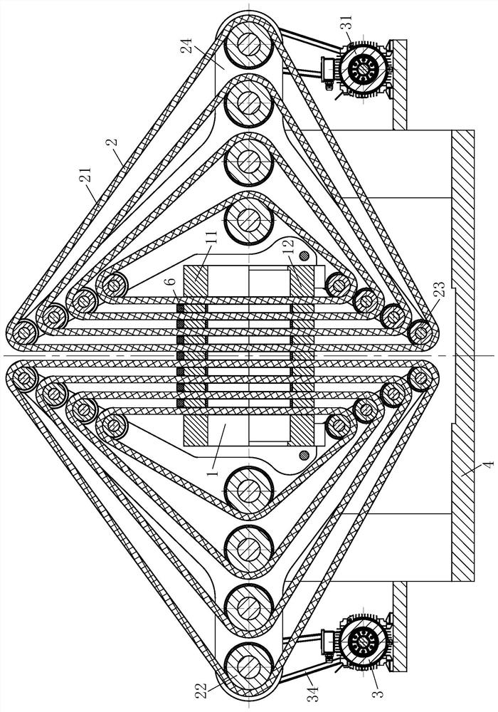
[0039] Such as Figure 1 to Figure 8 As shown, a batch polishing equipment for silicon wafers includes a clamping part 1, a polishing part 2, a power part 3 and a mounting frame 4; the clamping part 1 is arranged above the mounting frame 4; the clamping part 1 For clamping silicon wafers; the top of the mounting frame 4 is provided with a grinding part 2; the grinding part 2 is used to polish the surface of the silicon wafer; the mounting frame 4 is provided with the power part 3; The power unit 3 is used to provide power for the grinding unit 2;

[0040] The clamping part 1 includes an upper clamping body 11, a lower clamping body 12 and a No. 1 electric push rod 13; the upper clamping body 11 and the lower clamping body 12 are both semi-circula...


PUM


Abstract

The invention belongs to the technical field of semiconductor silicon wafers, and particularly relates to silicon wafer batch polishing equipment which comprises a clamping component, a polishing component, a power component and a mounting frame. A first electric push rod is controlled to retract to further drive an upper clamping body to rotate, then the upper clamping body is opened, then a silicon wafer to be machined is placed on a supporting strip, then the first electric push rod is controlled to stretch out to further drive the upper clamping body to rotate, so that the silicon wafer is clamped, then the power component drives a first belt wheel to rotate, so that a polishing belt is driven to move under the cooperation of the second belt wheel, the silicon wafer is subjected to a resultant force in the process that the polishing belt polishes the silicon wafer, so that the silicon wafer automatically rotates in an annular structure formed by the supporting strip and the clamping strip, the whole face is polished in the automatic rotation process of the silicon wafer, and meanwhile, the plurality of silicon wafers are polished, and therefore, batch polishing of the silicon wafers is realized.

Description

technical field [0001] The invention belongs to the technical field of semiconductor silicon wafers, in particular to a batch polishing equipment for silicon wafers. Background technique [0002] Elemental silicon is a gray, brittle, tetravalent, non-metallic chemical element. 27.8% of the earth's crust is composed of silicon, second only to oxygen, and silicon is a relatively abundant element in nature. Silicon is found in quartz, agate, flint and common beach rocks. Silicon wafers, also known as wafers, are processed from silicon ingots. Millions of transistors can be etched on silicon wafers through special processes, and are widely used in the manufacture of integrated circuits. [0003] The polishing process is divided into two steps, cutting and final polishing. Abrasion is the process of removing a thin layer of silicon to produce wafers with no surface damage. Final polishing does not remove any material other than the micropits created by the cutting process fro...

Claims


Application Information

Patent Timeline
IPC IPC(8): B24B21/04B24B21/18B24B9/06B24B47/12B24B55/03B24B55/06
CPCB24B9/065B24B21/04B24B21/18B24B47/12B24B55/03B24B55/06
Inventor 周勤
Owner 周勤
Why Eureka
Try Eureka