Display memory based on phase change material
A phase-change material and phase-change storage technology, which is applied in the field of functional semiconductors, can solve the problems of inconvenient large-area preparation of display units and cumbersome color rendering methods, and achieve the effects of low power consumption, fast conversion speed, and flexible form
- Summary
- Abstract
- Description
- Claims
- Application Information
AI Technical Summary
Problems solved by technology
Method used
Image

Examples
Embodiment 1
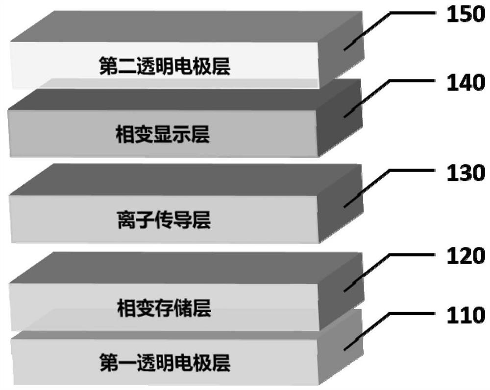
[0036]The glass substrate is ultrasonically cleaned in acetone, ethanol, and deionized water respectively, fixed on the substrate tray and placed in a magnetron sputtering equipment, and sputtered to form a transparent conductive material: the target material is ITO target material, the sputtering power supply is RF power supply, and the power density 3W / cm 2 , the atmosphere is pure argon, the pressure is 0.3Pa, and the sputtering time is 60min, the ITO conductive film with a smooth surface is obtained, the thickness is 100-200nm, and the measured surface resistance is 5-50Ω / cm 2 .
Embodiment 2
[0038] Formation of VO by sputtering on glass substrates sputtered with transparent conductive materials 2 Thin film: the target material is vanadium trioxide (V 2 o 3 ) target, the sputtering power supply adopts DC power supply, and the power density is 2.5W / cm 2 , the atmosphere is pure argon, the pressure is 1.5Pa, the sputtering time is 15min, and then vacuum annealed at 450°C for 5min to obtain VO with a smooth surface. 2 Thin film, the thickness of which is 50-100nm.
Embodiment 3
[0040] in VO 2 Aluminum silicate (Al x SiO y ) Ion-conducting layer film: the target material is aluminum silicate target material, the sputtering power supply is radio frequency power supply, and the power density is 2.5W / cm 2 , the atmosphere is pure argon, the pressure is 2.0Pa, and the room temperature sputtering time is 45 minutes, the aluminum silicate (Al x SiO y )film. The resulting aluminum silicate (Al x SiO y ) film thickness is 100-200nm, and the light transmittance between 380-760nm is greater than 85%.
PUM
| Property | Measurement | Unit |
|---|---|---|
| Thickness | aaaaa | aaaaa |
| Thickness | aaaaa | aaaaa |
| Thickness | aaaaa | aaaaa |
Abstract
Description
Claims
Application Information
 - R&D Engineer
- R&D Manager
- IP Professional
- Industry Leading Data Capabilities
- Powerful AI technology
- Patent DNA Extraction
Browse by: Latest US Patents, China's latest patents, Technical Efficacy Thesaurus, Application Domain, Technology Topic.
© 2024 PatSnap. All rights reserved.Legal|Privacy policy|Modern Slavery Act Transparency Statement|Sitemap