Semiconductor light-emitting element and preparation method thereof

A technology of light-emitting components and semiconductors, applied in semiconductor devices, electrical components, circuits, etc., can solve the problems of less research and application of plasmon effect, and achieve enhanced uniformity of light emission and anti-ESD ability, and improved mobility and distribution. chance, the effect of improving quantum efficiency

Active Publication Date: 2021-08-31
XIAMEN SILAN ADVANCED COMPOUND SEMICON CO LTD
View PDF4 Cites 1 Cited by
  • Summary
  • Abstract
  • Description
  • Claims
  • Application Information

AI Technical Summary

Problems solved by technology

However, the research and application of surface

Method used


Image

  • Semiconductor light-emitting element and preparation method thereof
  • Semiconductor light-emitting element and preparation method thereof
  • Semiconductor light-emitting element and preparation method thereof

Examples


Embodiment Construction

[0052] At present, the industry mainly focuses on improving the performance of light-emitting diodes such as brightness improvement, ESD and aging, while there are few researches and applications on the surface plasmon effect in light-emitting diodes.

[0053] Therefore, it is necessary to study the surface plasmon effect in light-emitting diodes to improve the performance of light-emitting diodes.

[0054] The invention provides a semiconductor light-emitting element, which utilizes the surface plasmon effect to improve the lateral expansion ability and vertical injection efficiency of holes, thereby improving the quantum efficiency, luminous uniformity and ESD resistance of the semiconductor light-emitting element.

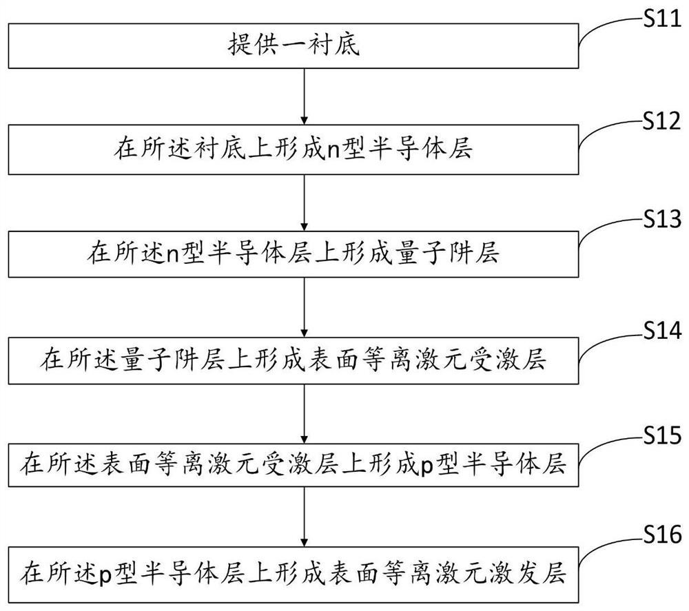
[0055] The semiconductor light-emitting element proposed by the present invention and its preparation method will be further described in detail below with reference to the accompanying drawings and specific examples. The advantages and features of the present i...


PUM

PropertyMeasurementUnit
Carrier concentrationaaaaaaaaaa
Thicknessaaaaaaaaaa
Thicknessaaaaaaaaaa

Abstract

The invention provides a semiconductor light-emitting element and a preparation method thereof. The semiconductor light-emitting element sequentially comprises a substrate, an n-type semiconductor layer, a quantum well layer and a p-type semiconductor layer from bottom to top, and further comprises a surface plasmon excited layer and a surface plasmon excitation layer, the quantum well layer is arranged on the p-type semiconductor layer, the surface plasmon excitation layer is arranged on the p-type semiconductor layer, and the surface plasmon excited layer is arranged between the quantum well layer and the p-type semiconductor layer and/or between the p-type semiconductor layer and the surface plasmon excitation layer. Through the surface plasmon excitation layer, the longitudinal hole injection efficiency and the transverse hole expansion capability of the two-dimensional hole gas of the surface plasmon excited layer can be induced and enhanced, the quantum efficiency of the semiconductor light-emitting element is improved, and the light-emitting uniformity and the ESD resistance of the semiconductor light-emitting element are enhanced.

Description

technical field [0001] The invention relates to the technical field of semiconductor optoelectronic devices, in particular to a semiconductor light-emitting element and a preparation method thereof. Background technique [0002] Nitride semiconductors are the third-generation compound semiconductors. Light-emitting elements made of this material have become the mainstream lighting source in the market because of their advantages such as energy saving and environmental protection, high luminous efficiency, easy adjustment of color wavelength, small size, and long service life. Since the wavelength of the nitride semiconductor is adjustable, it can cover yellow light, green light, blue light, purple light and deep ultraviolet band, so it is widely used in laser display, Mini-LED (Mini Light Emitting Diode, sub-millimeter light-emitting diode) backlight, Micro -LED (Micro Light Emitting Diode, miniature light-emitting diode) backlight, home lighting, outdoor street lighting, st...

Claims


Application Information

Patent Timeline
IPC IPC(8): H01L33/14H01L33/04H01L33/06H01L33/44H01L33/00
CPCH01L33/14H01L33/04H01L33/06H01L33/44H01L33/0075H01L33/007H01L2933/0025
Inventor 郑锦坚高默然毕京锋范伟宏李森林曾家明邬元杰张成军
Owner XIAMEN SILAN ADVANCED COMPOUND SEMICON CO LTD
Why Eureka
Try Eureka