Processing method of high aspect ratio metallized blind hole

A technology of metallized blind holes and processing methods, applied in the field of circuit board manufacturing, can solve the problems of poor hole consistency, small bottom of metallized blind holes, unprotected metallized blind holes, etc., to ensure qualified and consistent size sexual effect

Active Publication Date: 2022-08-02
珠海杰赛科技有限公司 +1
View PDF4 Cites 0 Cited by
  • Summary
  • Abstract
  • Description
  • Claims
  • Application Information

AI Technical Summary

Problems solved by technology

With the development of PCB in the direction of small size, light weight, three-dimensional installation and high connection reliability, the design of metallized blind holes has become more and more common. Process metallized blind holes. For the design of metallized blind holes with a thickness-to-diameter ratio greater than 0.8, especially the design of elongated holes, the metallized blind holes are not protected during the manufacturing process, and the top is easily attacked by etching. The bottom of the metallized blind hole is small, and the hole consistency is poor, which makes it difficult for the design of the metallized blind hole to meet customer requirements

Method used


Image

  • Processing method of high aspect ratio metallized blind hole

Examples


Embodiment Construction

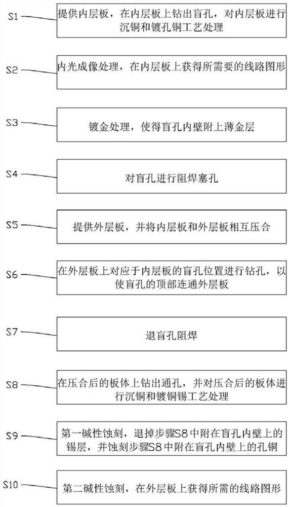
[0017] Embodiments of the present invention are described in detail below, referring to figure 1 , an embodiment of the present invention provides a processing method of a high aspect ratio metallized blind hole, comprising the following steps:

[0018] S1. Provide an inner layer board, and drill blind holes on the inner layer board, and process the inner layer board with copper immersion and plated hole copper, so that the blind hole is plated with copper layer, so that the upper and lower surfaces of the inner layer board can be connected;

[0019] S2, internal light imaging processing, obtain the required circuit pattern on the inner layer board, after the circuit pattern is made, the inner layer board is subjected to AOI inspection, and after the inspection is qualified, the next step is entered;

[0020] S3. Gold plating, so that a thin gold layer is attached to the inner wall of the blind hole to protect the copper layer plated in the blind hole;

[0021] S4. Solder th...


PUM

PropertyMeasurementUnit
thicknessaaaaaaaaaa

Abstract

The invention relates to the field of circuit board manufacturing, and discloses a processing method for metallized blind holes with high aspect ratio. Before the lamination process, gold plating is performed to protect the copper of the hole. During the process of making the through hole, the copper layer and tin layer will be plated in the blind hole again. The copper layer and the tin layer on the gold layer are removed during the process of caustic etching and the second alkaline etching. Under the protection of soft gold, the copper plated in the blind hole at the beginning will not be etched away. Before the pressing process, the blind holes are soldered and plugged to prevent glue overflowing in the holes during pressing. After pressing the inner layer board and the outer layer board, the solder mask in the holes is removed to complete the processing of metallized blind holes. , to ensure that the metallized blind holes are qualified, and the metallized blind holes have good dimensional consistency, which can meet the requirements of customers.

Description

technical field [0001] The invention relates to the field of circuit board manufacturing, in particular to a processing method of a high aspect ratio metallized blind hole. Background technique [0002] PCB, also known as printed circuit board, is a carrier for the electrical connection of electronic components to each other, and is an important electronic component. With the development of PCB in the direction of small size, light weight, three-dimensional installation and high connection reliability, the design of metallized blind holes has become more and more common. Process metallized blind holes. For the design of metallized blind holes with an aspect ratio greater than 0.8, especially the design of slender holes, in the process of processing, the metallized blind holes cannot be protected, and the top is easily attacked by etching. The bottom of the metallized blind hole is small, and the consistency of the holes is poor, which makes the design of the metallized blin...

Claims


Application Information

Patent Timeline
Patent Type & Authority Patents(China)
IPC IPC(8): H05K3/46H05K3/42H05K3/00
CPCH05K3/4623H05K3/4614H05K3/429H05K3/0094
Inventor 徐梦云关志锋李超谋刘国汉房鹏博
Owner 珠海杰赛科技有限公司
Why Eureka
Try Eureka