Biomask and method for patterning on substrate

A mask and patterning technology, which is applied in the photoengraving process of the pattern surface, the originals and instruments for photomechanical processing, etc., can solve the problem of high price

Active Publication Date: 2021-09-07
SOUTH UNIVERSITY OF SCIENCE AND TECHNOLOGY OF CHINA
View PDF8 Cites 0 Cited by
  • Summary
  • Abstract
  • Description
  • Claims
  • Application Information

AI Technical Summary

Problems solved by technology

However, the mask plates of TSV technology and MIVs technology are mainly divided into four typ

Method used


Image

  • Biomask and method for patterning on substrate

Examples


Embodiment 1

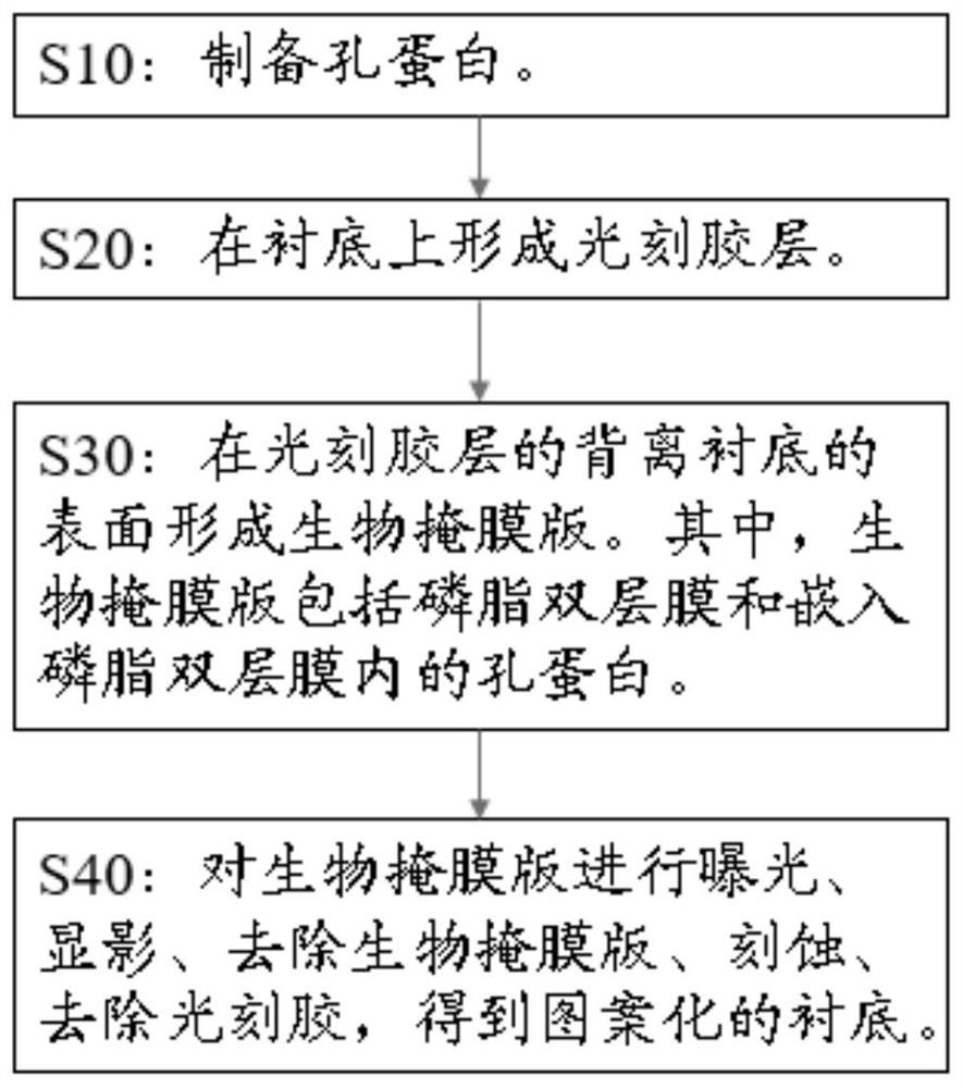
[0082] This embodiment provides a method for preparing a monolithic interlayer through hole, including the following steps:

[0083] (1) Select a silicon wafer with a crystal phase of and a thickness of 50 μm, with a dense silicon dioxide layer of 10 nm thick on the surface, and clean the silicon wafer according to the RCA standard process flow.

[0084] According to the coating speed of 3000rpm, the coating acceleration of 2000rpm / s, and the coating time of 20s, the above-mentioned cleaned silicon wafers were coated with a positive photoresist. After the coating is completed, it is dried at a temperature of 100°C for 180s.

[0085] (2), immerse the silicon wafer with the photoresist layer in the NHS / EDC mixture (2.0mmol / LNHS+1.0mmol / L EDC) to activate for 10min, then immerse it in the 0.1mol / L avidin solution for protein Fixed for 5 minutes. Spin-coat 1ml of DPPC vesicle solution on the surface of the silicon wafer after protein immobilization at a spin-coating speed of 20...

Embodiment 2

[0090] The difference between Example 2 and Example 1 is that the porin is PlyAB.

[0091] In this embodiment, the line width of the through hole on the silicon chip can be as low as 14nm.

Embodiment 3

[0093] The difference between Example 3 and Example 1 is that the vesicle solution is clathrin-coated vesicle solution.

[0094] In this embodiment, the line width of the through hole on the silicon chip can be as low as 7nm.


PUM

PropertyMeasurementUnit
Thicknessaaaaaaaaaa

Abstract

The invention relates to a biomask and a method for patterning on a substrate, and belongs to the technical field of integrated circuit preparation. A method of patterning on a substrate includes the steps: forming a photoresist layer on the substrate; forming a biological mask on the surface, deviating from the substrate, of the photoresist layer; exposing and developing the biological mask, removing the biological mask, etching, and removing the photoresist to obtain the patterned substrate, wherein the biomask comprises a phospholipid double-layer membrane and pore protein embedded in the phospholipid double-layer membrane. In the application, the mask used when patterning is carried out on the substrate is the biological mask, and the pattern is formed through the pore protein, so the process cost can be effectively reduced.

Description

technical field [0001] The present application relates to the technical field of integrated circuit preparation, and in particular to a biological mask and a patterning method on a substrate. Background technique [0002] With the continuous breakthrough of integrated semiconductor manufacturing process technology, the performance of integrated circuit devices has developed rapidly, and the corresponding microelectronic packaging technology has gradually become an important factor restricting the development of semiconductor technology. In order to realize smaller size, faster processing speed and lower manufacturing cost of semiconductor devices. More and more advanced packaging technologies that go beyond traditional packaging concepts have been proposed. Among them, the three-dimensional packaging technology realizes interconnection and communication through interlayer interconnection, which effectively shortens the interconnection length, reduces the parasitic parameter...

Claims


Application Information

Patent Timeline
IPC IPC(8): H01L21/027G03F1/76
CPCH01L21/0274G03F1/76
Inventor 叶怀宇王少刚高宸山杨荟茹刘起鹏张国旗
Owner SOUTH UNIVERSITY OF SCIENCE AND TECHNOLOGY OF CHINA
Why Eureka
Try Eureka