

Formation method of semiconductor structure
A semiconductor and gate structure technology, applied in the field of semiconductor structure formation, can solve problems such as poor semiconductor performance and poor sidewall morphology
- Summary
- Abstract
- Description
- Claims
- Application Information
AI Technical Summary
Problems solved by technology
Method used
Image

Examples
Embodiment Construction
[0033] As mentioned in the background, existing semiconductor structures perform poorly.
[0034] The reasons for the poor performance of the semiconductor structure will be described in detail below in conjunction with the accompanying drawings. Figure 1 to Figure 4 It is a structural schematic diagram of each step of a method for forming a semiconductor structure.
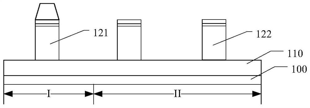
[0035] Please refer to figure 1 , providing a substrate 100, the substrate 100 includes a first region I and a second region II, the first region I and the second region II have fins 110 thereon, and the first region I has fins 110 across the fins. The first gate structure 121 of the fin portion 110, the second region II has a second gate structure 122 across the fin portion 110, and the first gate structure 121 has an interface layer 125 thereon.
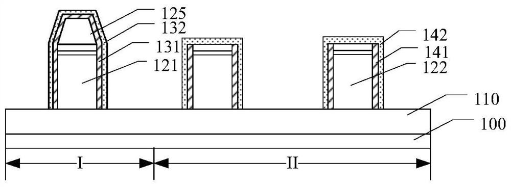
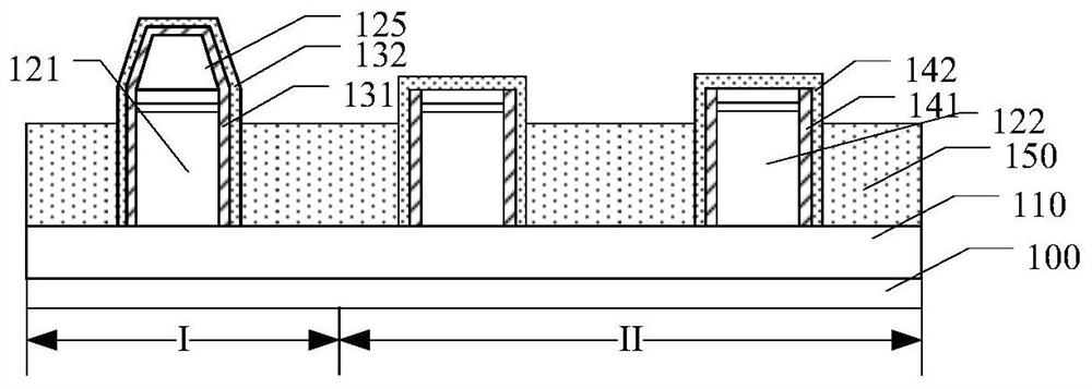
[0036] Please refer to figure 2 , forming an initial first sidewall structure on the surface of the first grid structure 121, the initial first sidewall structur...
PUM
 Abstract
Description
Claims
Application Information