Electronic component X-ray inspection defect automatic identification method

An electronic component, automatic recognition technology, applied in neural learning methods, character and pattern recognition, instruments, etc., can solve the problem of few component chip image detection methods

Pending Publication Date: 2021-09-17
CHINA ELECTRONICS STANDARDIZATION INST +1
View PDF5 Cites 1 Cited by
  • Summary
  • Abstract
  • Description
  • Claims
  • Application Information

AI Technical Summary

Problems solved by technology

[0006] At present, the defect detection of electronic components in China mainly focuses on the related research of printed circuit board (PCB) solder joint defect detection, mounted component detection and SMT surface packaging, etc., and the detection of component chip images few methods

Method used


Image

  • Electronic component X-ray inspection defect automatic identification method
  • Electronic component X-ray inspection defect automatic identification method
  • Electronic component X-ray inspection defect automatic identification method

Examples


Embodiment Construction

[0046] In order to further explain the technical means and functions adopted by the present invention to achieve the intended purpose, the present invention will be described in detail below in conjunction with the accompanying drawings and preferred embodiments.

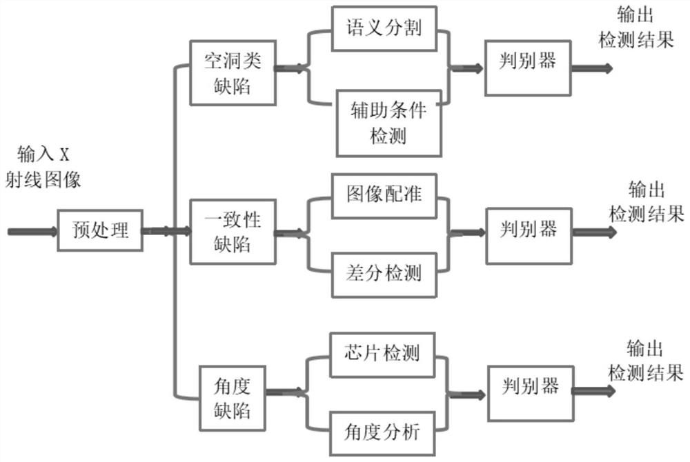
[0047] In an embodiment of the present invention, a method for automatic identification of defects in X-ray inspection of electronic components, such as figure 1 shown. The flow of the automatic detection algorithm for X-ray defects of electronic components is as follows:

[0048] Step 1: Perform preprocessing such as denoising and enhancement on the X-ray image;

[0049] Preprocessing is the primary link in various image analysis and recognition. Due to the particularity of the imaging principle, the main problem faced in the analysis and recognition of X-ray images is low contrast, so the pre-processing link in the early stage is mainly based on contrast enhancement. According to the typical characteristics of ...


PUM


Abstract

The invention discloses an electronic component X-ray inspection defect automatic identification method. The method comprises the following steps: preprocessing an X-ray image; marking a sample manually in a semi-automatic or automatic manner, and dividing defect types of to-be-detected electronic components into three types, namely cavity defects, consistency defects and angle defects, according to the packaging and defect forms of electronic components; and detecting four types of cavity defects by using a semantic segmentation method based on a convolutional neural network. The convolutional neural network is trained through a large number of samples, accurate segmentation of various cavity defects is realized, and the automatic defect identification efficiency is greatly improved. Meanwhile, a welding area, a sealing area and the like of a chip are detected through a gray projection method, and the qualification of the chip is judged according to corresponding judgment criteria. The problems that automatic calculation cannot be carried out and judgment is carried out purely by manpower in the prior art are solved, and the interference problem of cavities in a welding interface of a substrate and a tube shell in a hybrid integrated circuit is solved.

Description

technical field [0001] The invention relates to the technical field of automatic identification of defects in X-ray inspection of electronic components, in particular to a method for automatic identification of defects in X-ray inspection of electronic components. Background technique [0002] Military electronic components are the basic components of national defense military electronic systems, mainly including microelectronic devices such as semiconductor discrete devices and integrated circuits, as well as special devices such as relays and sensors. Military electronic components are the material guarantee of information systems such as nuclear, aviation, aerospace, ships, weapons, and electronics. Their stability and reliability directly affect the functions and performance indicators of information systems. [0003] Packaging defects of military electronic components is one of the main factors affecting their quality. X-ray inspection is a means of non-destructive tes...

Claims


Application Information

Patent Timeline
Patent Type & Authority Applications(China)
IPC IPC(8): G06T7/00G06T7/11G06T7/62G06K9/62G06N3/04G06N3/08G06T5/00G06T5/40
CPCG06T7/0004G06T7/11G06T7/62G06T5/002G06T5/007G06T5/40G06N3/08G06T2207/10116G06T2207/30148G06T2207/30204G06T2207/20081G06T2207/20084G06N3/045G06F18/2431
Inventor 黄东巍王爽王素玉张玉芹周钦沅张宏宇麻力
Owner CHINA ELECTRONICS STANDARDIZATION INST
Why Eureka
Try Eureka