

A high-frequency-band dielectric material characteristic measurement method
A technology of dielectric materials and measurement methods, applied in special data processing applications, design optimization/simulation, etc., can solve the problems of expensive spread spectrum modules of terahertz vector network analyzers, and achieve controllable test costs, convenient and accurate acquisition, and low cost cheap effect
- Summary
- Abstract
- Description
- Claims
- Application Information
AI Technical Summary
Problems solved by technology
Method used
Image

Examples
Embodiment 1
[0027] An embodiment of the present invention is a method for measuring the characteristics of a high-frequency dielectric material, comprising the following steps:
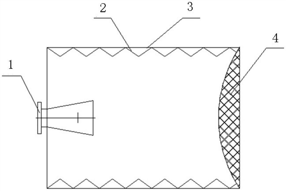
[0028] 1. Establish in the three-dimensional full-wave electromagnetic simulation software (such as HFSS, CST Microwave Studio, etc.) figure 1 The lens antenna model shown, and its first simulation.
[0029] The lens antenna model includes an illumination feed 1 , a support structure 2 and a lens 3 made of high-frequency dielectric material. Preferably, in another embodiment, the illumination feed 1 is a rectangular horn antenna with a medium gain (gain of 10-15dBi), which is used to confine the energy transmitted from the standard rectangular waveguide to radiate space. The supporting structure 2 is a hollow cavity whose main function is to fix the relative positional relationship between the illumination feed source 1 and the lens 3 , and may be a hollow cavity such as a cuboid or a cylinder, for example. The...
Embodiment 2
[0035] In another embodiment, the high-frequency dielectric material to be measured is polytetrafluoroethylene, and its test frequency range is 216±1 GHz. The lens 3 is processed into a lens form with a thick middle and a thin periphery by using the dielectric material, and is installed at the tail of the support structure 2 . The support structure 2 and the irradiation feed source 1 are designed and processed with copper materials. The length of the support structure 2 along the beam irradiation direction is 58mm, and the size of the mouth surface of the installation lens 3 is 33mm×19mm. The gain of illumination feed 1 is designed to be 15dBi, and the input electrical interface is WR-4 waveguide international standard interface. The lens 3 made of the high-frequency dielectric material to be measured further focuses the electromagnetic wave emitted by the irradiation feed 1 to increase the overall gain of the lens antenna and improve the accuracy of the medium measurement. T...
PUM
 Abstract
Description
Claims
Application Information