A detection method and detection structure of a display backplane

A display backplane and detection method technology, applied in semiconductor/solid-state device testing/measurement, electrical components, circuits, etc., can solve problems such as complicated and inconvenient operation, increased time cost, dead pixels, etc., to achieve accurate and efficient detection methods, Simple steps and time-saving effect

Active Publication Date: 2022-05-27
CHONGQING KONKA PHOTOELECTRIC TECH RES INST CO LTD
View PDF7 Cites 0 Cited by
  • Summary
  • Abstract
  • Description
  • Claims
  • Application Information

AI Technical Summary

Problems solved by technology

[0003] However, the contact electrode pairs on the display backplane may have dead spots during the manufacturing process, resulting in defects in the display effect of the final display panel. It is complicated and inconvenient to operate by emitting light to judge whether there are dead pixels, and repeated soldering of LED chips increases the difficulty of operation and increases the time cost

Method used


Image

  • A detection method and detection structure of a display backplane
  • A detection method and detection structure of a display backplane
  • A detection method and detection structure of a display backplane

Examples


Embodiment Construction

[0032] In order to make those skilled in the art better understand the solutions of the present invention, the technical solutions in the embodiments of the present invention will be clearly and completely described below with reference to the accompanying drawings in the embodiments of the present invention. Obviously, the described embodiments are only These are some embodiments of the present invention, but not all embodiments. Based on the embodiments of the present invention, all other embodiments obtained by those of ordinary skill in the art without creative efforts shall fall within the protection scope of the present invention.

[0033] In the prior art, Micro LED displays, as the mainstream of new types of displays, have good stability, long life, and advantages in operating temperature. At the same time, they also inherit the low power consumption, color saturation, and fast response speed of LEDs. , strong contrast and other advantages, has great application prospe...


PUM


Abstract

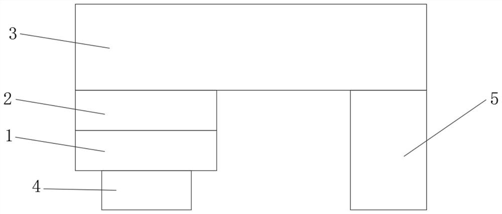
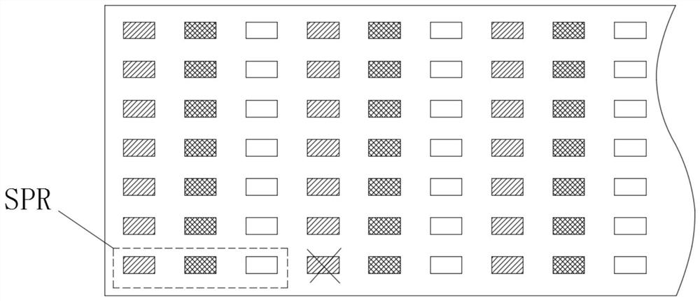
The invention discloses a detection method and a detection structure of a display backplane, wherein a display backplane is provided, and multiple groups of contact electrode pairs are arranged on the display backplane, and the contact electrode pairs include input electrodes and output electrodes; A detection structure, the detection structure includes a plurality of light-emitting parts, and a plurality of detection circuits, at least one of the light-emitting parts is arranged between every two detection circuits, and the detection circuit is used to guide the light-emitting parts Power-on signal; assemble the detection structure on the display backplane, so that one detection circuit is simultaneously connected to the input electrode in one group of the contact electrode pair and the other adjacent contact electrode The output electrodes in the pair are connected; output driving electrical signals to the display backplane; if the light-emitting element does not emit light, it is determined that the group of contact electrode pairs to which the input electrodes connected to the detection circuit belong is dead point. The present application quickly judges whether the display backplane is damaged or not by observing the luminescence of the luminous parts.

Description

technical field [0001] The present invention relates to the technical field of display devices, and in particular, to a detection method and a detection structure of a display backplane. Background technique [0002] At present, the use of electronic products in people's daily life is extremely common, and the technology of electronic display screens is constantly being developed and innovated. The maturity of Light Emitting Diode (LED) technology has further promoted the use of display panels, especially the use of Micro LED displays. Use gradually to occupy the market. In the prior art, contact electrode pairs are formed on the display backplane, and LED chips are welded on the contact electrode pairs to form a display panel. [0003] However, the contact electrode pair on the display backplane may have dead points during the manufacturing process, resulting in defects in the display effect of the final display panel. The existing Micro LED display panel testing methods m...

Claims


Application Information

Patent Timeline
Patent Type & Authority Patents(China)
IPC IPC(8): H01L21/66
CPCH01L22/34H01L22/12
Inventor 王广徐瑞林林建宏
Owner CHONGQING KONKA PHOTOELECTRIC TECH RES INST CO LTD
Why Eureka
Try Eureka