

Lithographic equipment and silicon wafer pre-alignment method
A lithography equipment and pre-alignment technology, which is applied in optics, instruments, photoplate-making process of patterned surface, etc., can solve the problems of low efficiency, affecting the movement travel time and station handover efficiency, time-consuming problems, etc., to achieve Reduce process time, improve handover efficiency and flexibility, and improve efficiency
- Summary
- Abstract
- Description
- Claims
- Application Information
AI Technical Summary
Problems solved by technology
Method used
Image

Examples
Embodiment Construction
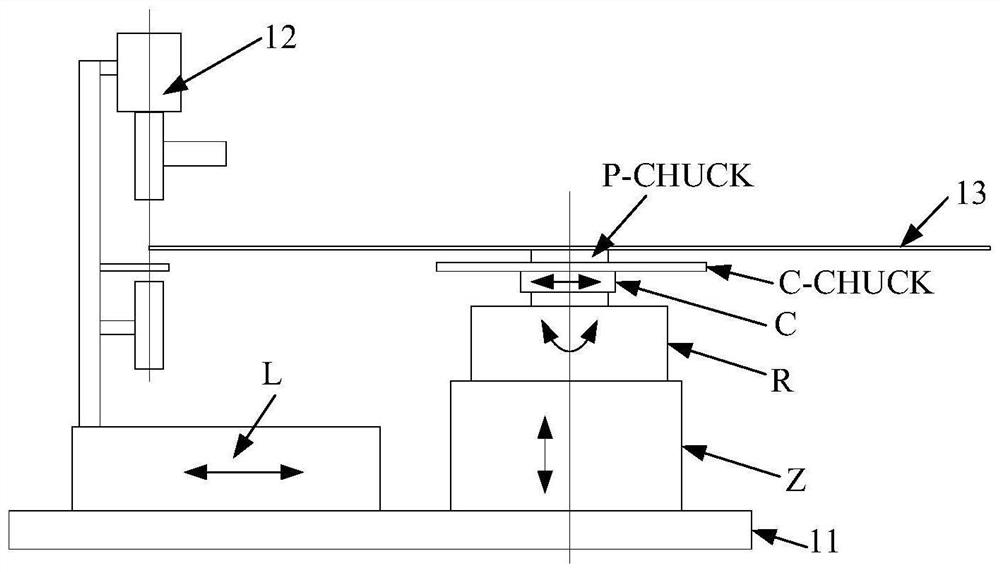
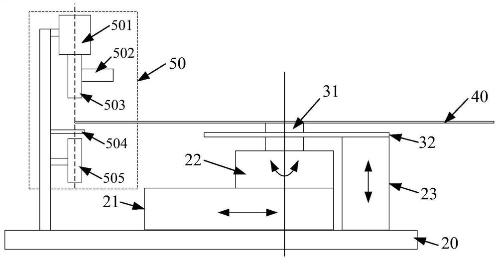
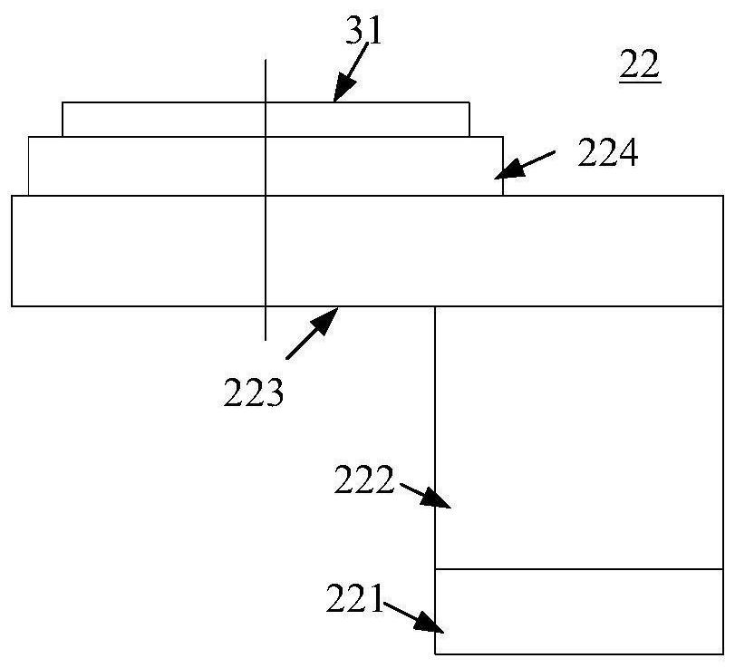
[0040] Based on the above research, an embodiment of the present invention provides a photolithography apparatus, especially a silicon wafer pre-alignment device and a pre-alignment method therein. The present invention will be described in further detail below in conjunction with the accompanying drawings and specific embodiments. The advantages and features of the present invention will become clearer from the following description. It should be noted that the drawings are all in a very simplified form and use imprecise scales, and are only used to facilitate and clearly assist the purpose of illustrating the embodiments of the present invention.
[0041]An embodiment of the present invention provides a lithography equipment, including: an exposure device, a mask table device, a workpiece table device, and a silicon wafer transmission device; wherein the silicon wafer transmission device includes a silicon wafer pre-alignment device, and the silicon wafer The pre-alignment ...
PUM
 Abstract
Description
Claims
Application Information