Photoelectric detector, arithmetic processor with memory function and preparation method
A photodetector and computing processor technology, applied in the field of detectors, can solve problems such as inability to perform logical operations on two pictures
- Summary
- Abstract
- Description
- Claims
- Application Information
AI Technical Summary
Problems solved by technology
Method used
Image
Examples
preparation example Construction
[0050] The preparation method of MoxWySz alloy thin film of the present invention, described confinement oblique CVD method comprises the steps:
[0051] S1 Mix the tungsten source and NaCl in proportion, put them evenly on the precursor substrate, and place the precursor substrate in the quartz boat one; the preferred source of Wu is WO 3 .
[0052] In a preferred embodiment, WO 3 Mix with NaCl in a ratio of 10:1, place evenly on the precursor substrate, and place the substrate in a 1-inch quartz boat;
[0053] S2 places the molybdenum source and NaOH on the front end of the precursor substrate; the molybdenum source is preferably MoO 3 .
[0054] In a preferred embodiment, a molybdenum source and a trace amount of NaOH whose mass is half that of the tungsten source are placed on the front end of the precursor substrate;
[0055] S3 will be Si / SiO 2 The growth substrate is placed face down and obliquely above the precursor substrate; thereby achieving confinement; confin...
Embodiment 1
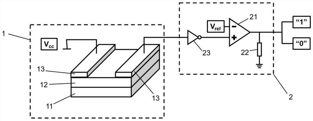
[0088] This embodiment provides a photodetector 1, such as figure 1 As shown, the photodetector 1 includes a substrate layer 11 and a photoresponsive layer 12 from bottom to top; wherein, the photoresponsive layer 12 is a defect-rich transition metal sulfide Mo x W 1-x S 2 Alloy thin film; an electrode layer 13 is set on the photoresponsive layer 12 .
[0089] Here, the material of the substrate layer 11 is a silicon wafer with a silicon oxide layer.
[0090] The material of the electrode layer 13 is Ti / Au, and the thickness is 5nm / 50nm.
[0091] The preparation process of the photodetector 1 is:
[0092] Step 1: Providing Si / SiO 2 Precursor substrates and Si / SiO 2 growth substrate;
[0093] Step 2: Put the WO 3 Mix with NaCl in a ratio of 10:1, place evenly on the precursor substrate, and place the substrate in a 1-inch quartz boat;
[0094] Step 3: Convert the mass to WO 3 half of MoO 3 and a trace amount of NaOH are placed on the front end of the precursor substr...
Embodiment 2
[0103] This embodiment provides an image logic operation processor unit with a memory function, such as figure 1 As shown, it includes a photodetector 1 and a comparator module 2, wherein the photodetector 1 sequentially includes a substrate layer 11 and a photoresponse layer 12 from bottom to top; wherein the photoresponse layer 12 is defect-rich Transition metal sulfide Mo x W 1-x S 2 Alloy thin film; an electrode layer 13 is set on the photoresponsive layer 12 . The comparator module 2 includes a voltage comparator 21 , a resistor 22 and a transimpedance amplifier 23 .
[0104] Here, the material of the substrate layer 11 is generally a silicon wafer with a silicon oxide layer.
[0105] The material of the electrode layer 13 is Ti / Au, and the thickness is 5nm / 50nm.
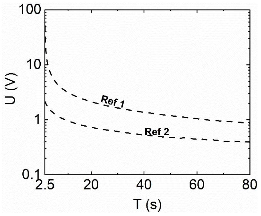
[0106] Described voltage comparator 21 is the general voltage comparator 21 that market is general, its reference voltage V ref For the preset voltage value Ref 1 or Ref 2 ( figure 2 ); the resistance v...
PUM
| Property | Measurement | Unit |
|---|---|---|
| thickness | aaaaa | aaaaa |
| electrical resistance | aaaaa | aaaaa |
Abstract
Description
Claims
Application Information

