Palladium-doped carbon film/oxide/semiconductor material with photoconductive effect

A semiconductor and oxide technology, applied in the field of palladium-doped carbon film/oxide/semiconductor materials, can solve problems such as unfavorable applications, and achieve good application value, abundant reserves, and cheap prices

Inactive Publication Date: 2011-10-12
CHINA UNIV OF PETROLEUM (EAST CHINA)
View PDF5 Cites 7 Cited by
  • Summary
  • Abstract
  • Description
  • Claims
  • Application Information

AI Technical Summary

Problems solved by technology

An order of magnitude of low photoconductivity variation is clearly not conducive to practical applications

Method used


Image

  • Palladium-doped carbon film/oxide/semiconductor material with photoconductive effect
  • Palladium-doped carbon film/oxide/semiconductor material with photoconductive effect
  • Palladium-doped carbon film/oxide/semiconductor material with photoconductive effect

Examples


Embodiment Construction

[0018] The present invention will be described in detail below in conjunction with the accompanying drawings and embodiments.

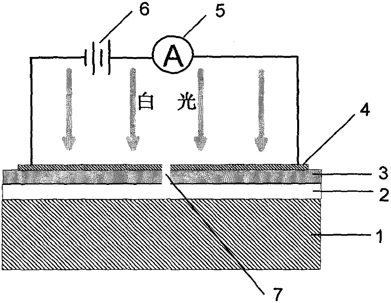
[0019] In an embodiment, graphite powder with a purity of 99.9% is mixed with palladium powder with a purity of 99.9%, and a palladium-carbon composite target with a palladium atomic number content of 1% is produced by cold pressing. The palladium-carbon composite target is sputtered onto a silicon wafer 1 with a thickness of 1.0 mm to retain a natural oxide layer 2 by magnetron sputtering. The thickness of silicon dioxide 2 is about 1.2 nanometers, forming a silicon wafer on the silicon wafer. Layer thickness is the palladium-doped carbon film 3 of 100 nanometers, on the palladium-doped carbon film 3, one layer of translucent copper film 4 is sputtered, and the copper film 4 is used as upper electrode, in order to prevent that the copper film is directly conducted and designed a spacer 7 (spacer Zone 7 divides the copper film and the carbon film into...


PUM

PropertyMeasurementUnit
thicknessaaaaaaaaaa
thicknessaaaaaaaaaa
currentaaaaaaaaaa

Abstract

The invention provides a palladium-doped carbon film / oxide / semiconductor material with a photoconductive effect, which is characterized in that graphite composite targets which are doped with atomicity contents being 0-5% of palladium are sputtered on a 0.5-1.0mm-thick semiconductor substrate with oxides to form a film with 20-200nanometer in thickness so as to prepare the palladium-doped carbon film / oxide / semiconductor material. The palladium-doped carbon film / oxide / semiconductor material has the photoconductive effect and a good linear relation between light current and light radiation intensity exists, thus the palladium-doped carbon film / oxide / semiconductor material can be used to manufacture optoelectronic sensors. The optoelectronic sensors can operate at room temperature, are simple in structure and low in cost, the production technology is simple and the rate of finished products is high, and the optoelectronic sensors have wide application prospects.

Description

technical field [0001] The invention relates to a palladium-doped carbon film / oxide / semiconductor material with photoconductive effect. Background technique [0002] A photosensitive sensor is a sensor that can quickly convert the received light signal into a corresponding electrical signal. The material with this function is called a photosensitive material, and the device made is called a photosensitive device. Photosensitive devices include photoresistors, photodiodes, and phototransistors. Photosensitive devices can be used to control various devices or actuators such as alarms, testers, automatic switches, relays, etc. in the form of visible light or infrared light. Therefore, photosensitive devices are widely used in various automatic control circuits, household appliances and various measuring instruments. Under the action of light, the photosensitive material absorbs the incident photon energy. If the photon energy is greater than or equal to the forbidden band wid...

Claims


Application Information

Patent Timeline
Patent Type & Authority Applications(China)
IPC IPC(8): H01L31/08H01L31/0352H01L31/18
CPCY02P70/50
Inventor 王盛薛庆忠马明李建鹏甄玉花
Owner CHINA UNIV OF PETROLEUM (EAST CHINA)
Why Eureka
Try Eureka