Hybrid packaging device based on spot size transformation and grating coupling

A grating coupling and hybrid packaging technology, applied in the directions of light guides, optics, optical components, etc., can solve the problems of small alignment tolerance, large package size, low coupling efficiency, etc., to achieve small overall size and improve alignment tolerance. , the effect of improving the optical coupling efficiency

Pending Publication Date: 2021-10-08
INST OF SEMICONDUCTORS - CHINESE ACAD OF SCI
View PDF6 Cites 2 Cited by
  • Summary
  • Abstract
  • Description
  • Claims
  • Application Information

AI Technical Summary

Problems solved by technology

The efficiency of optical coupling will directly determine the performance of silicon-based chips. At present, mature optical coupling methods have small alignment tolerances, low coupling efficiency, and large packaging device sizes.

Method used


Image

  • Hybrid packaging device based on spot size transformation and grating coupling
  • Hybrid packaging device based on spot size transformation and grating coupling

Examples


Embodiment Construction

[0022] Hereinafter, an embodiment of the present disclosure will be described with reference to the accompanying drawings. It should be understood, however, that these descriptions are merely exemplary, and not to limit the scope of the disclosure. In the following detailed description, many of the specific details are set forth to provide a comprehensive understanding of the embodiments of the present disclosure. However, it is apparent that one or more embodiments may be implemented without these specific details. Further, in the following description, a description of the well-known structure and techniques is omitted to avoid unnecessarily obscuring the concepts of the present disclosure.

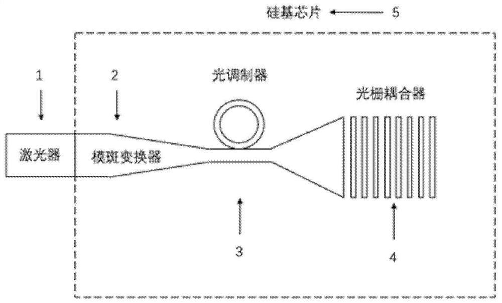
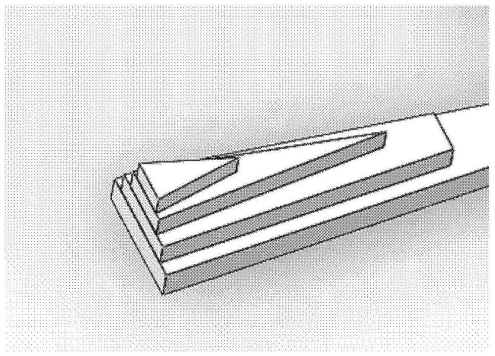
[0023] Light coupling is generally divided into two types, which are direct coupling and indirect coupling, and indirect coupling is not conducive to large scale integration. The use of direct coupling is a more mature is to use a mold converter and a grating coupler. Although the mutant co...


PUM


Abstract

The invention provides a hybrid packaging device based on spot size transformation and grating coupling. The hybrid packaging device comprises a silicon-based chip; a spot size converter which is integrated on the silicon-based chip and is used for realizing the optical mode conversion and coupling of optical signals; an optical modulator which is integrated on the silicon optical chip, is connected with the spot-size converter and a grating coupler, and is used for modulating the optical signals; the grating coupler which is integrated on the silicon-based chip and is used for realizing the coupling of optical signals and changing the optical direction, wherein the grating coupler comprises a waveguide structure and a grating structure, and the conical waveguide structure is connected with the spot size converter.

Description

Technical field [0001] The present invention relates to the field of optoelectronic integration techniques, and more particularly to a hybrid package device based on mold transform and grating coupling. Background technique [0002] In the backbone network and the next generation data center, the electronic chip encounters the rate bottleneck, and the photoconographic chip has the focus of development due to its low power consumption and high bandwidth characteristics. For large-scale multi-channel photon integrated chips, silicon-based light electronic chips have significant advantages, and the maturation process of using silicon-based chips is an inevitable trend in single-chip integration and reduction in volume. The optical coupling efficiency will directly determine the performance of the silicon-based chip, the current mature optical coupling method is small, the coupling efficiency is low, and the package device is large. Therefore, it is found to have an efficient optical...

Claims


Application Information

Patent Timeline
Patent Type & Authority Applications(China)
IPC IPC(8): G02B6/12G02B6/122G02B6/124
CPCG02B6/12004G02B6/12002G02B6/1228G02B6/124G02B2006/12085G02B2006/12107G02B2006/12142G02B2006/12152
Inventor 翟鲲鹏陈寅芳李明祝宁华
Owner INST OF SEMICONDUCTORS - CHINESE ACAD OF SCI
Why Eureka
Try Eureka