Optical proximity correction method and device

A technology of optical proximity correction and lithography, which is applied in optics, original parts and instruments for opto-mechanical processing, etc., and can solve the problems that the lithography process window cannot be guaranteed and the process quality cannot be guaranteed.

Pending Publication Date: 2021-10-12
CHANGXIN MEMORY TECH INC
View PDF5 Cites 1 Cited by
  • Summary
  • Abstract
  • Description
  • Claims
  • Application Information

AI Technical Summary

Problems solved by technology

The existing OPC is mainly to ensure that the critical dimensions of the silicon wafer are close to the design target and minimize the edge placement error (Edge PlacementError, EPE), but at this time it may not be possible to ensure that the size of the photolithography process window (Process window, PW) conforms to the process The scope of the above requirements, resulting in the quality of the process cannot be guaranteed

Method used


Image

  • Optical proximity correction method and device
  • Optical proximity correction method and device
  • Optical proximity correction method and device

Examples


Embodiment Construction

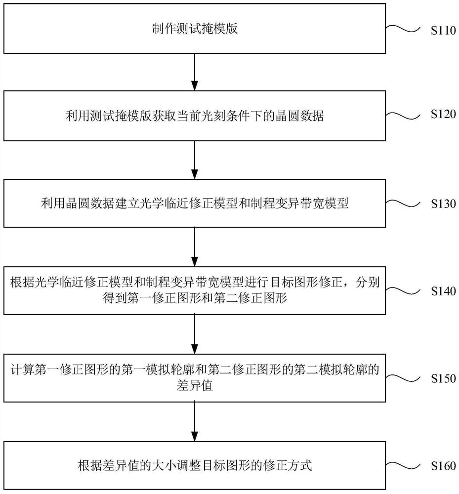
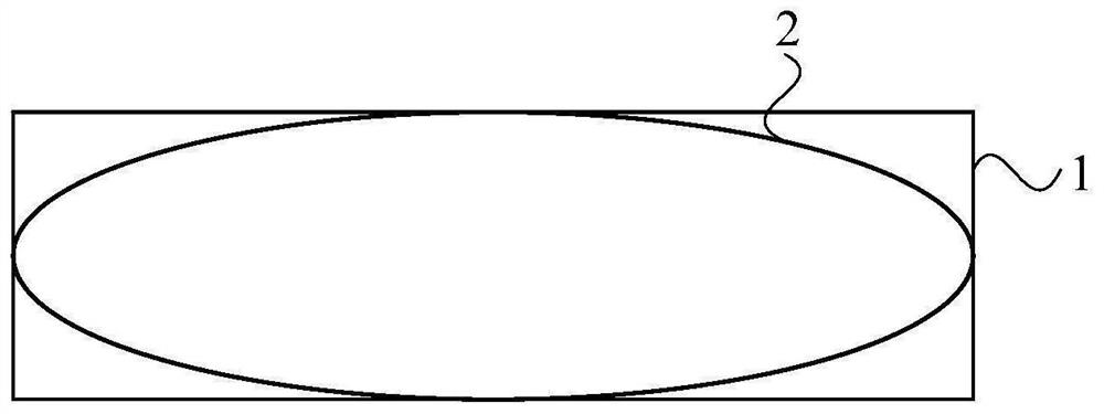
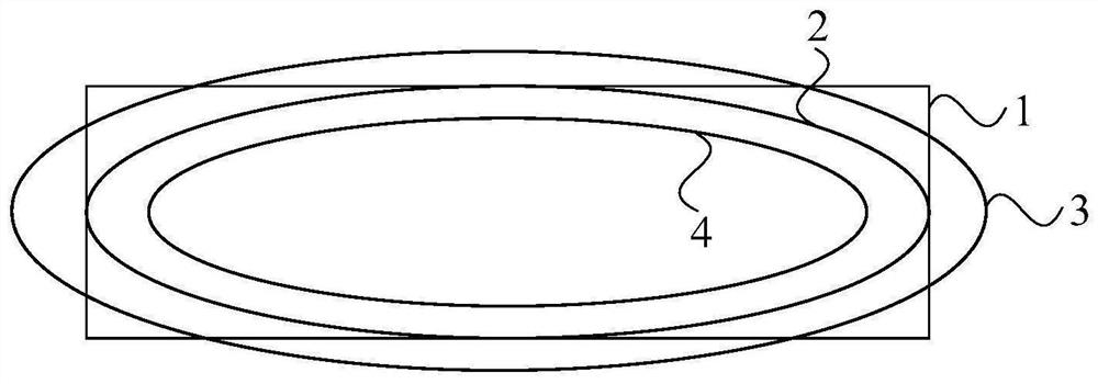
[0053] The present invention will be further described in detail below in conjunction with the accompanying drawings and embodiments. It should be understood that the specific embodiments described here are only used to explain the present invention, but not to limit the present invention. In addition, it should be noted that, for the convenience of description, only some structures related to the present invention are shown in the drawings but not all structures.

[0054]Terms used in the embodiments of the present invention are only for the purpose of describing specific embodiments, and are not intended to limit the present invention. It should be noted that the orientation words such as "up", "down", "left", and "right" described in the embodiments of the present invention are described from the angles shown in the drawings, and should not be interpreted as a reference to the implementation of the present invention. Example limitations. Also in this context, it also need...


PUM


Abstract

The embodiment of the invention discloses an optical proximity correction method and device. The optical proximity correction method comprises the following steps: manufacturing a test mask; obtaining wafer data under the current photoetching condition by using the test mask; establishing an optical proximity correction model and a process variation bandwidth model by using wafer data; correcting the target graph according to the optical proximity correction model and the process variation bandwidth model to respectively obtain a first corrected graph and a second corrected graph; calculating a difference value between a first simulation contour of the first correction graph and a second simulation contour of the second correction graph; and adjusting the correction mode of the target graph according to the size of the difference value. According to the technical scheme provided by the embodiment of the invention, variation possibly caused by the process variation bandwidth is considered during correction, a photoetching process window is enlarged, and the yield of products is improved.

Description

technical field [0001] Embodiments of the present invention relate to semiconductor manufacturing technology, and in particular to an optical proximity correction method and device. Background technique [0002] Due to the diffraction effect of ultraviolet light, the image pattern exposed on the photoresist on the surface of the silicon wafer is distorted, and the image quality is finally reduced. This is called the optical proximity effect (Optical Proximity Effect, OPE). The image distortion caused by OPE is mainly The performance is that the line width is shifted, the lines are shortened, and the corners are rounded. [0003] By making appropriate modifications to the pattern on the mask to compensate for this effect, the same pattern as the design can be obtained on the silicon wafer. This correction is called Optical Proximity Correction (OPC). The existing OPC is mainly to ensure that the critical dimensions of the silicon wafer are close to the design target and mini...

Claims


Application Information

Patent Timeline
IPC IPC(8): G03F1/36
CPCG03F1/36G03F7/70441Y02D10/00
Inventor 陈信廷
Owner CHANGXIN MEMORY TECH INC
Why Eureka
Try Eureka