System-in-package and manufacturing method of the same

a technology of system-in-package and manufacturing method, which is applied in the direction of semiconductor devices, semiconductor/solid-state device details, electrical apparatus, etc., can solve the problems of time-consuming manufacturing process, inability to meet the demand of producing smaller chips with high density elements on the chip, and complicated semiconductors, etc., to achieve the effect of improving reliability, yield and reducing the total thickness of the packag

Active Publication Date: 2009-12-31
ADL ENERGY CORP
View PDF9 Cites 67 Cited by
  • Summary
  • Abstract
  • Description
  • Claims
  • Application Information

AI Technical Summary

Benefits of technology

[0009]The object of the present invention is to provide a manufacturing method of a System-in-Package (SIP) with a planarized substrate to improve the reliability, yield and to reduce the total thickness of the package.
[0010]Another object of the present invention is to provide a manufacturing method of a System-in-Package (SIP) which can use photolithography process without consideration of modification of process parameters to solve difficulties caused by the surface topology.

Problems solved by technology

As a semiconductor become more complicated, the traditional package technique, for example lead frame package, flex package, rigid package technique, can't meet the demand of producing smaller chip with high density elements on the chip.
Furthermore, because conventional package technologies have to divide a dice on a wafer into respective dice and then package the die respectively, therefore, these techniques are time consuming for manufacturing process.
Since the chip package technique is highly influenced by the development of integrated circuits, therefore, as the size of electronics has become demanding, so does the package technique.
Another prior art, superfine-circuit semiconductor package structure disclosed by Patent Publication Number US 20080006936 still suffers the planarity issue.
Both of the prior arts, the substrate with through hole used as embedded substrate will suffer poor yield due to lack of planarity.
Further, it will cause photolithograph problems in the subsequent processing.
This may conflict with the demand of reducing the size of a chip.
Further, the prior art suffers complicated process to form the “Panel” type package.
It is unlikely to control the surface of die and compound at same level due to warp after heat curing the compound, the CMP process may be needed to polish the uneven surface.
The cost is therefore increased.

Method used


Image

  • System-in-package and manufacturing method of the same
  • System-in-package and manufacturing method of the same
  • System-in-package and manufacturing method of the same

Examples


Embodiment Construction

[0018]The invention will now be described in greater detail with preferred embodiments of the invention and illustrations attached. Nevertheless, it should be recognized that the preferred embodiments of the invention is only for illustrating. Besides the preferred embodiment mentioned here, present invention can be practiced in a wide range of other embodiments besides those explicitly described, and the scope of the present invention is expressly not limited expect as specified in the accompanying Claims.

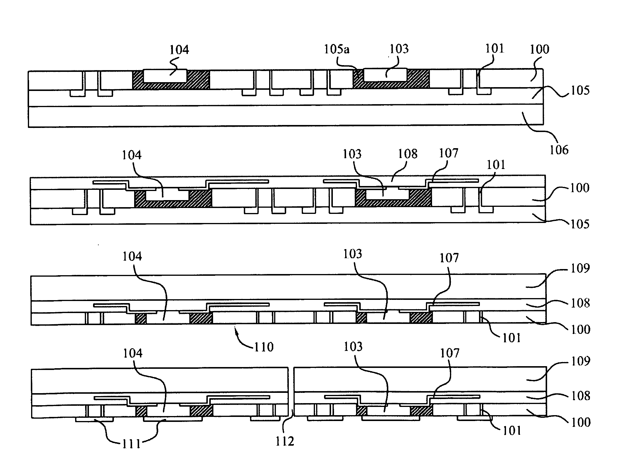
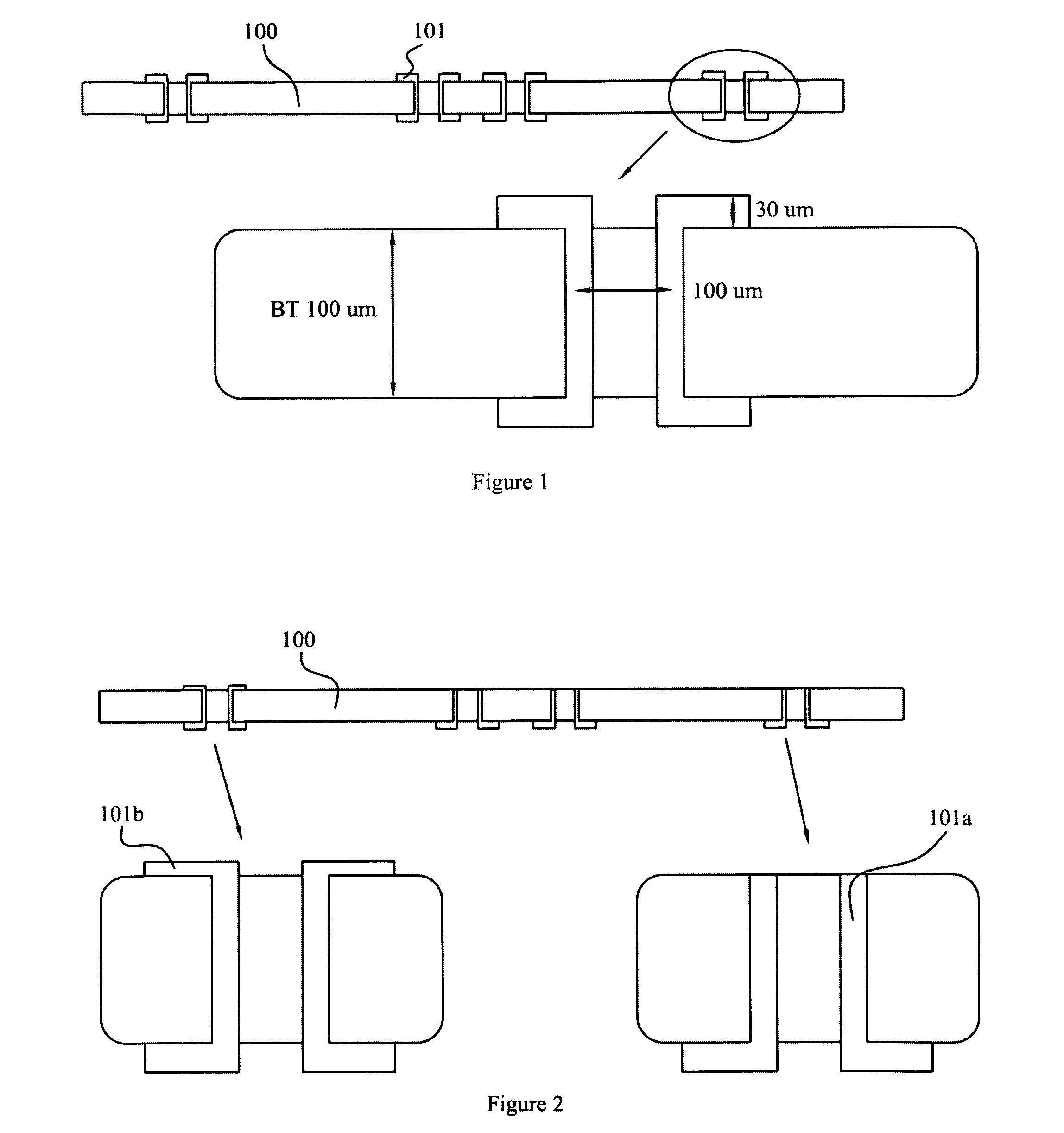
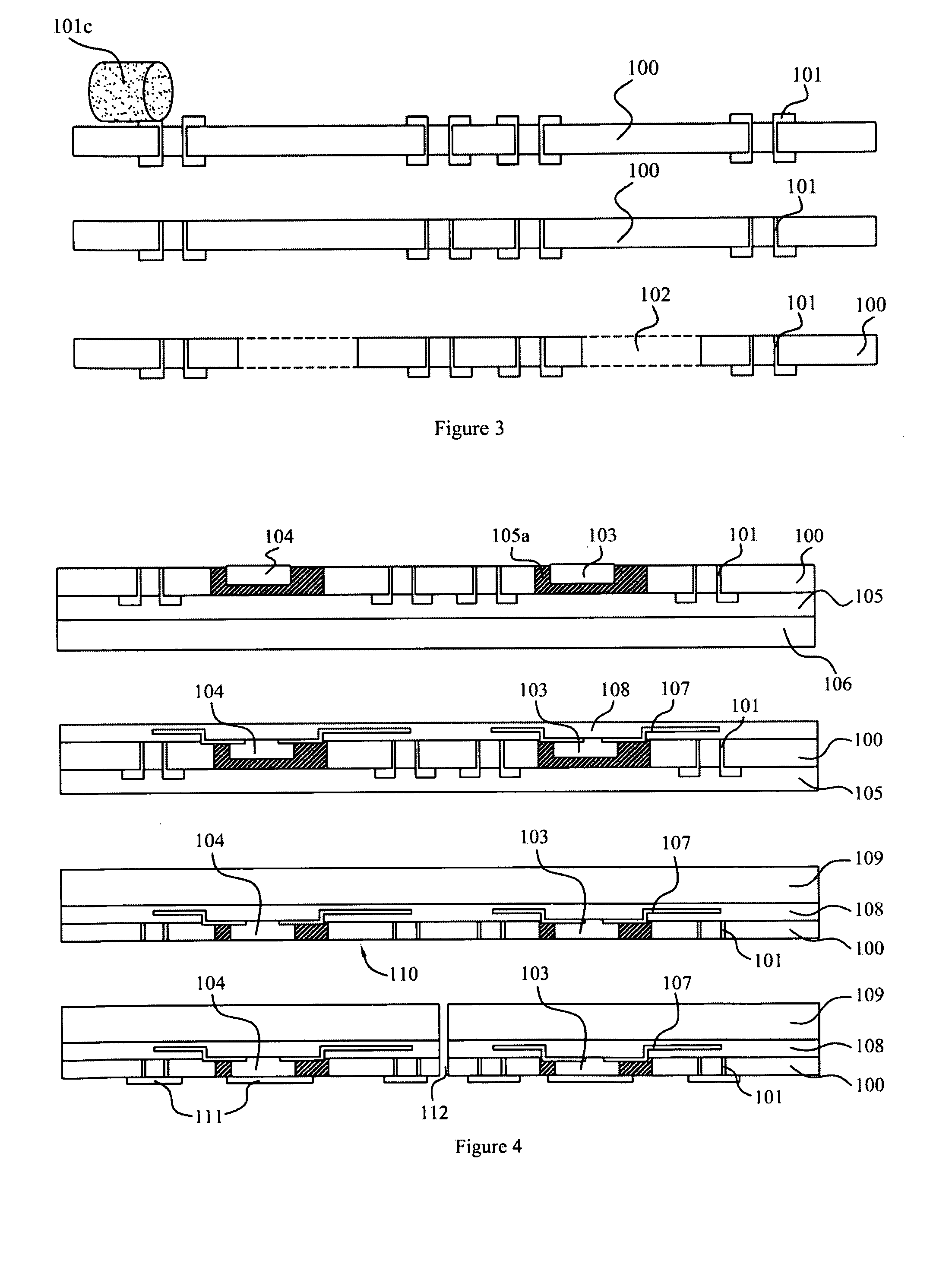
[0019]The present invention discloses a structure of System-in-Package (SIP) and manufacturing method thereof which utilizing a planarized substrate as starting substrate by grinding the back side of the substrate and die to expose back side of the die and form a super thin structure. Connectors are disposed at the back side of the die and substrate, for example under bump metallurgy (UBM), which connects the solder joint and the chip, is formed onto the back side of the die and / o...


PUM


Abstract

The present invention discloses a structure of package comprising: a substrate with a die receiving through hole and a contact conductive via formed therein, a die disposed within the die receiving through hole, a surrounding material filled in the gap except the die area of the die receiving though hole, a re-distribution layer formed on the substrate and coupled to the contact conductive via, a protection layer formed over the re-distribution layer, a cover material formed over the protection layer; and a terminal contact pad formed on the lower surface of the substrate and under the contact conductive via and the die to couple the contact conductive via.

Description

FIELD OF THE INVENTION [0001]This invention relates to a semiconductor package structure, and more particularly to a manufacturing method of a System-in-Package (SIP) with a planarized substrate to improve the reliability, yield and to reduce the thickness of the package.DESCRIPTION OF THE PRIOR ART [0002]In the field of semiconductor devices, the device density is increased and the device dimension is reduced, continuously. The demand for the packaging or interconnecting techniques in such high density devices is also increased to fit the situation mentioned above. Conventionally, in the flip-chip attachment method, an array of solder bumps is formed on the surface of the die. The formation of the solder bumps may be carried out by using a solder composite material through a solder mask for producing a desired pattern of solder bumps. The function of chip package includes power distribution, signal distribution, heat dissipation, protection and support . . . and so on. As a semicon...

Claims


Application Information

Patent Timeline
Patent Type & Authority Applications(United States)
IPC IPC(8): H01L23/48H01L21/52
CPCH01L23/5389H01L24/18H01L2224/18H01L2924/01013H01L2924/01029H01L2924/01075H01L2924/01082H01L2924/09701H01L2924/01006H01L2924/01033H01L2924/01079H01L2924/14H01L2924/3511H01L2924/3512H01L21/568H01L24/19H01L24/97H01L2224/04105H01L2224/06181H01L2224/24227H01L2924/18162H01L2924/00
Inventor HU, DYI-CHUNGYU, CHUN-HUI
Owner ADL ENERGY CORP
Why Eureka
Try Eureka