
Light-emitting diode with latticed metal film and preparation method thereof

A technology of light-emitting diodes and metal films, which is applied in the direction of electrical components, circuits, semiconductor devices, etc., can solve the problems of current congestion and low light utilization rate, and achieve the effects of increasing conductivity, improving uniformity, and reducing surface roughness and scattering

Inactive Publication Date: 2021-10-12
SHENZHEN INST OF WIDE BANDGAP SEMICON
View PDF5 Cites 0 Cited by
  • Summary
  • Abstract
  • Description
  • Claims
  • Application Information

AI Technical Summary

Problems solved by technology

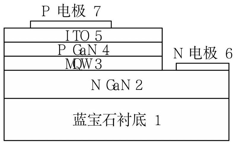
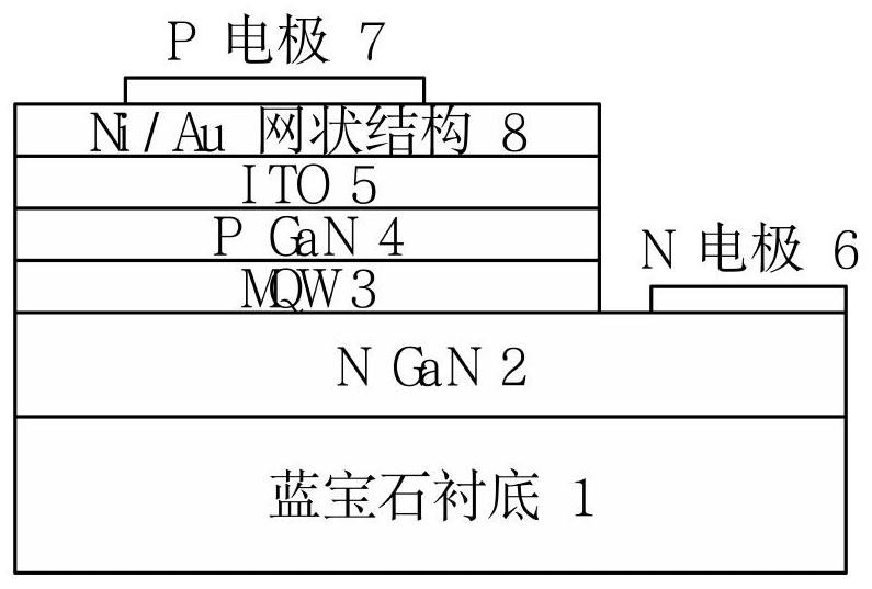
[0004] In order to solve the problems of current crowding caused by the lateral flow of LED chip current in a lateral structure and low utilization rate of light due to the blocking of light by the front electrode, the present invention proposes an LED device structure that is conducive to current transmission. The technical solution is specifically: a A light-emitting diode with a grid-shaped metal film, the structure includes a substrate, an N-type GaN layer, a quantum well layer, a P-type quantum well layer, and a transparent conductive layer from bottom to top; the transparent conductive layer is formed with a porous belt. A mesh metal film; a P electrode is formed on the mesh structure, and an N electrode is formed on the N-type GaN layer

Method used


Image

  • Light-emitting diode with latticed metal film and preparation method thereof
  • Light-emitting diode with latticed metal film and preparation method thereof
  • Light-emitting diode with latticed metal film and preparation method thereof

Examples


Embodiment 1

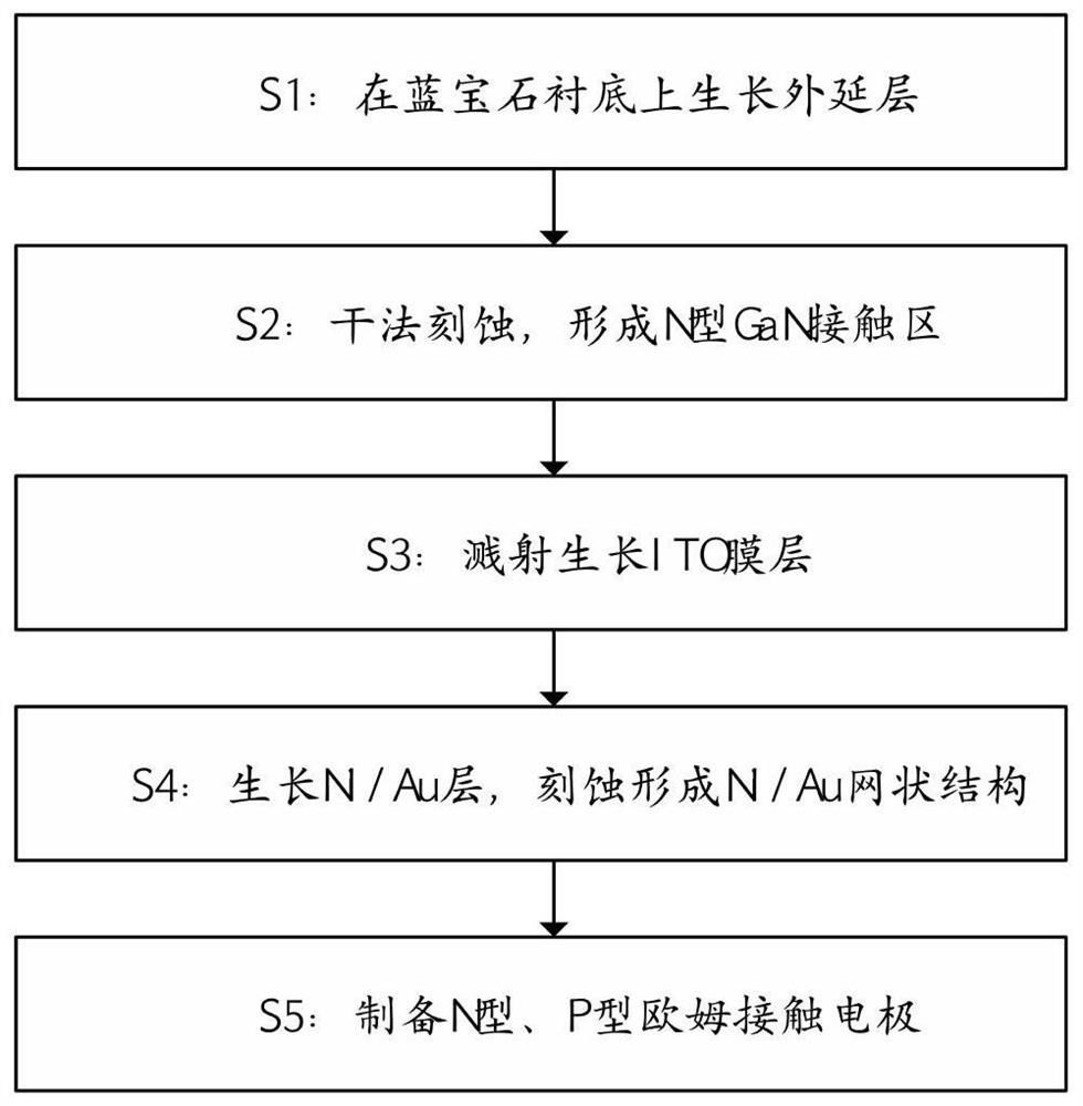
[0030] Embodiment 1: This embodiment provides a light-emitting diode with a grid-shaped metal film and a preparation method thereof, and the specific steps include:

[0031] S1 grow epitaxial layer on sapphire substrate

[0032] Such as Figure 4 As shown, an N-type GaN layer 2 and a P-type GaN layer 4 are epitaxially grown sequentially using MOCVD equipment on a sapphire substrate. Quantum well layer 3 is formed between N-type GaN layer 2 and P-type GaN layer 4 .

[0033] S2 dry etching to form N-type GaN contact area

[0034] Such as Figure 5 As shown, after applying glue and developing the photolithographic hard film, use the photoresist as a mask to etch P-type GaN, and the etching gas is Cl 2 / Ar / BCl 3 , so that the surface of the N-type GaN is exposed.

[0035] S3 sputtering growth of ITO film layer

[0036] Such as Figure 6 As shown, using the DC magnetron sputtering method, using the linear continuous coating machine to sputter and grow the ITO film layer, th...


PUM

PropertyMeasurementUnit
thicknessaaaaaaaaaa
thicknessaaaaaaaaaa
pore sizeaaaaaaaaaa

Abstract

The invention provides a light-emitting diode with a latticed metal film and a preparation method thereof. The light-emitting diode structurally comprises a substrate, an N-type GaN layer, a quantum well layer, a P-type quantum well layer and a transparent conductive layer in sequence from bottom to top, and a porous net-shaped metal film with bulges is formed on the transparent conductive layer; and a P electrode is formed on the latticed structure, and an N electrode is formed on the N-type GaN layer. According to the LED device structure beneficial to current transmission provided by the invention, the external quantum efficiency of light is improved on the basis of keeping the advantages of simple preparation process and convenient transverse integration, and the problems of current crowding and low light utilization rate of a common transverse structure LED device are solved. The mesh electrode is prepared in a Stepper photoetching mode, the mesh structure can be extended to more places with the same electrode pin area, current transmission is facilitated, and the uniformity of current on a chip is improved.

Description

technical field [0001] The invention belongs to the technical field of light-emitting devices, and in particular relates to a light-emitting diode with a grid-shaped metal film and a preparation method thereof. Background technique [0002] LED chips have two basic structures: horizontal and vertical. The lateral structure LED chip means that the two electrodes of the chip are on the same side of the epitaxial wafer, and since the electrodes are on the same side, the current flows laterally in the n- and p-type confinement layers. On the contrary, the vertical structure LED chip means that two electrodes are distributed on different sides of the epitaxial wafer, and the patterned electrode and all the p-type confinement layers are used as the second electrode, so that the current flows almost all vertically through the LED epitaxial layer, and rarely flows laterally. current. The lateral structure LED chip also has the advantages of simple preparation structure, mature pro...

Claims


Application Information

Patent Timeline
Patent Type & Authority Applications(China)
IPC IPC(8): H01L33/44H01L33/14H01L33/38H01L33/00
CPCH01L33/44H01L33/14H01L33/38H01L33/007H01L2933/0016H01L2933/0025
Inventor 聂大伟闫春辉申广汤艳龙
Owner SHENZHEN INST OF WIDE BANDGAP SEMICON
Learn More