Electron beam lithography auxiliary process manufacturing method

A technology of electron beam lithography and manufacturing method, which is applied in the direction of semiconductor/solid-state device manufacturing, circuits, electrical components, etc., can solve the problems that affect the final device performance, production yield, unstable metal shape, collapse, etc., to avoid T Gate collapse, improve process yield, and reduce the effect of impact

Active Publication Date: 2021-10-19
XIAMEN SANAN INTEGRATED CIRCUIT
View PDF5 Cites 0 Cited by
  • Summary
  • Abstract
  • Description
  • Claims
  • Application Information

AI Technical Summary

Problems solved by technology

However, during the process of depositing metal, due to the stress, the photoresist is deformed and the shape of the T-shaped gate pattern changes, which will lead to the final deposited metal shape being very unstable and prone to collapse after peeling off. , which affects the performance of the final device and the production yield

Method used


Image

  • Electron beam lithography auxiliary process manufacturing method
  • Electron beam lithography auxiliary process manufacturing method
  • Electron beam lithography auxiliary process manufacturing method

Examples


Embodiment Construction

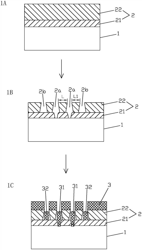
[0024] The present invention will be further explained below in conjunction with the accompanying drawings and specific embodiments. The drawings of the present invention are only schematic diagrams for easier understanding of the present invention, and their specific proportions can be adjusted according to design requirements. Those skilled in the art should understand the upper and lower relationships of relative components and the definition of front / back in the figures described herein refer to the relative positions of the components, so they can be turned over to present the same components, which should all belong to this document. The scope disclosed in the manual.

[0025] refer to figure 1 , the specific steps of an electron beam lithography-assisted process manufacturing method of an embodiment will be described below.

[0026] refer to figure 1 A, sequentially coating the first photoresist layer 21 and the second photoresist layer 22 on the semiconductor substr...


PUM

PropertyMeasurementUnit
thicknessaaaaaaaaaa

Abstract

The invention discloses an electron beam lithography auxiliary process manufacturing method, which comprises the following steps of forming a laminated layer of a first photoresist layer and a second photoresist layer on a semiconductor substrate, and carrying out electron beam exposure and development on the photoresist laminated layer to obtain a T-shaped pattern and auxiliary patterns positioned on two sides of the T-shaped pattern, wherein the exposure depth of the T-shaped pattern is the thickness of the first photoresist layer and the second photoresist layer, and the exposure depth of the auxiliary pattern is the thickness of the second photoresist layer, and then depositing metal and stripping photoresist to obtain T-shaped gate metal. Through the arrangement of the auxiliary pattern, the deformation quantity of the photoresist around the T-shaped pattern in the metal deposition process is reduced, the influence on the T-shaped gate morphology caused by the deformation of the photoresist is reduced, and the stability of the T-shaped gate metal morphology is improved.

Description

technical field [0001] The invention relates to the technical field of semiconductors, in particular to an electron beam lithography-assisted process manufacturing method. Background technique [0002] During the manufacturing process of the T-shaped gate of semiconductor devices, two layers of photoresist are usually used to achieve different photolithographic areas to obtain the pattern of the T-shaped gate, and then metal is deposited in the pattern to form a T-shaped gate metal structure, and then the photoresist is stripped. . However, during the process of depositing metal, due to the stress, the photoresist is deformed and the shape of the T-shaped gate pattern changes, which will lead to the final deposited metal shape being very unstable and prone to collapse after peeling off. , affecting the performance and production yield of the final device. Contents of the invention [0003] The purpose of the present invention is to overcome the deficiencies in the prior ...

Claims


Application Information

Patent Timeline
Patent Type & Authority Applications(China)
IPC IPC(8): H01L21/027H01L21/033H01L21/28
CPCH01L21/0277H01L21/0332H01L21/0337H01L21/28008
Inventor 杨宇林科闯何知逸李云燕
Owner XIAMEN SANAN INTEGRATED CIRCUIT
Why Eureka
Try Eureka