Metal capacitor structure and preparation method thereof

A metal capacitor and capacitor structure technology, applied in capacitors, circuits, electrical components, etc., can solve the problems of chip failure, poor reliability, easy breakdown of metal capacitor structures, etc., and achieve the effect of improving the breakdown voltage.

Active Publication Date: 2021-10-19
GUANGZHOU CANSEMI TECH INC
View PDF11 Cites 4 Cited by
  • Summary
  • Abstract
  • Description
  • Claims
  • Application Information

AI Technical Summary

Problems solved by technology

Wherein the thickness and the width of the relative interlayer dielectric layer 22 between the bottom metal layer 21 and the top metal layer 23 determine the capacitance value of the metal capacitor structure, the thinner the thickness of the dielectric layer, the larger the capacitance value, but the impact of the metal capacitor structure The lower the breakdown voltage, the worse the reliability under the working voltage (characterized by time-dependent dielectric breakdown TDDB). TDDB is one of the reliability indicators for evaluating the quality of the dielectric layer. A constant voltage is applied to both ends of the metal capacitor structure. Make the metal capacitor structure in the accumulation state, after a period of time, the dielectric layer will break down, this period of time is the life of the metal capacitor structure under this condition, if the TDDB performance of the metal capacitor structure declines, then the metal capacitor structure is easy to break down chip failure

Method used


Image

  • Metal capacitor structure and preparation method thereof
  • Metal capacitor structure and preparation method thereof
  • Metal capacitor structure and preparation method thereof

Examples


preparation example Construction

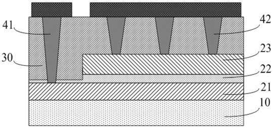
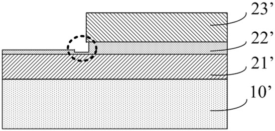
[0038] figure 2 It is a schematic cross-sectional view of forming a depression in the preparation method of the metal capacitor structure. Please refer to figure 2 , a bottom metal layer 21', an interlayer dielectric layer 22' and a top metal layer 23' are formed on the substrate 10', since the interlayer dielectric layer 22' determines the capacitance value of the metal capacitance structure, if the interlayer dielectric layer 22' If the defect density is low, the breakdown voltage of the metal capacitor structure is mainly limited by the etching of the top metal layer 23 ′. During the fabrication of the metal capacitor structure, it is necessary to use a patterned photoresist layer (not shown in the figure) as a mask to etch the top metal layer 23' to form an opening through the top metal layer 23', which exposes the interlayer The surface of the dielectric layer 22'. However, in order to completely remove the top layer metal layer 23' in the opening without residue, ge...


PUM


Abstract

The invention provides a metal capacitor structure and a preparation method thereof. The structure is characterized by comprising a substrate, a capacitor structure, a plurality of openings, a recess, and a side wall; the capacitor structure comprises a bottom metal layer, an interlayer dielectric layer and a top metal layer which are sequentially stacked on the substrate; the plurality of openings penetrate through the top metal layer and extend downwards into the interlayer dielectric layer; the recess is positioned on the side wall of the opening and extends downwards into the interlayer dielectric layer from the bottom of the opening; and the side wall is located in the opening and extends downwards from the side wall of the top metal layer to fill the recess; The breakdown voltage of the metal capacitor structure is improved.

Description

technical field [0001] The invention relates to the technical field of semiconductors, in particular to a metal capacitor structure and a preparation method thereof. Background technique [0002] Metal-insulator-metal (MIM), due to its small parasitic resistance, is widely used in analog circuits and radio frequency circuits. Different application requirements have different requirements for the parasitic resistance of metal capacitors. If it is used in radio frequency circuits, due to the high frequency (GHz), its capacitive reactance is low, and the total impedance of the parasitic resistance in the entire metal capacitor is high, which needs to be reduced as much as possible. However, for low-frequency analog circuits, such as in the application of panel driver chips, metal capacitors are used as storage for charge pumps, which require a higher breakdown voltage, and the corresponding time-dependent dielectric breakdown of metal capacitors (Time Dependent Dielectric Brea...

Claims


Application Information

Patent Timeline
Patent Type & Authority Applications(China)
IPC IPC(8): H01L49/02
CPCH01L28/40
Inventor 刘翔王家玺
Owner GUANGZHOU CANSEMI TECH INC
Why Eureka
Try Eureka