Method and device for increasing scanning angle of optical phased array

An optical phased array, scanning angle technology, applied in optics, nonlinear optics, instruments, etc., can solve problems such as increasing the complexity of the control system and operating costs, slowing down the speed of beam scanning, and low integration of array antennas. Achieve the effect of easy on-chip system integration, reduced optical path, and guaranteed speed

Pending Publication Date: 2021-10-22
HUAZHONG UNIV OF SCI & TECH
View PDF15 Cites 0 Cited by
  • Summary
  • Abstract
  • Description
  • Claims
  • Application Information

AI Technical Summary

Problems solved by technology

However, the scanning of the laser radar beam mainly depends on the diffraction output of the grating in the array antenna. The diffraction angle is mainly affected by the inherent parameters of the grating, and the scanning range is limited; The integration of the antenna is low; at the same time, the phase difference between the adjacent waveguides of the array antenna needs to be controlled during the scanning process, and the system is complex
In the existing technology, multiple two-dimensional optical phased arrays or antenna array units are mainly used to expand the scanning range and achieve full coverage of the scanning area, which not only increases the volume of the device, but also increases the complexity of the control system and running costs, but also slows down beam scanning

Method used


Image

  • Method and device for increasing scanning angle of optical phased array
  • Method and device for increasing scanning angle of optical phased array
  • Method and device for increasing scanning angle of optical phased array

Examples


Embodiment Construction

[0052] In order to make the object, technical solution and advantages of the present invention clearer, the present invention will be further described in detail below in conjunction with the accompanying drawings and embodiments. It should be understood that the specific embodiments described here are only used to explain the present invention, not to limit the present invention. In addition, the technical features involved in the various embodiments of the present invention described below can be combined with each other as long as they do not constitute a conflict with each other.

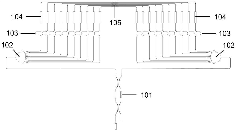
[0053] The invention provides a method and device for increasing the scanning angle of an optical phased array to realize the function of large-angle two-dimensional light beam scanning. Such as figure 1 As shown, the composition of the optical phased array device of the present invention mainly includes a broadband optical switch 101 , two power dividers 102 , two phase compensation regions 10...


PUM


Abstract

The invention discloses a method and a device for increasing the scanning angle of an optical phased array. The method comprises the following steps: a beam splitting step: splitting an input light beam into two paths of light beams with equal power; a longitudinal direction light beam scanning step: firstly, controlling the two paths of light beams to interfere constructively at an output end, and outputting from one path; then, performing optical path compensation on multiple paths of light beams with equal power to enable the initial phases of the light beams to be the same before diffraction output; and finally, changing the phase difference between adjacent light paths to realize transverse scanning of the emergent light beam at a certain longitudinal angle; a longitudinal reverse light beam scanning step: controlling the two paths of light beams to cancel interference at the same output end, and outputting the two paths of light beams from the other path; and repeating the steps to realize scanning of the emergent light beam in the longitudinal reverse direction. By means of the method and system, two-dimensional large-angle scanning can be achieved, and the longitudinal scanning angle is doubled; meanwhile, a device control system is simple, small in size, easy for system-on-chip integration and suitable for large-scale production and application.

Description

technical field [0001] The invention belongs to the field of optical phased array and laser radar, and more specifically relates to a method and device for improving the scanning angle of optical phased array. Background technique [0002] The rise of intelligent systems such as self-driving cars and intelligent robots has drawn attention to lidar systems. For lidar, fast and accurate beam scanning in a large area is a prerequisite for its commercial use. Optical phased array is a kind of light emitting device. By effectively adjusting the antenna, beam scanning can be realized. This device has a wide range of applications in lidar, and can also be used in optical imaging and military defense fields . [0003] Optical phased array devices based on waveguide technology have smaller size, lower power consumption and faster scanning speed, making them attract much attention in the fields of lidar, free space optical communication, and optical imaging and display. However, th...

Claims


Application Information

Patent Timeline
IPC IPC(8): G02F1/29G02F1/295G02F1/313
CPCG02F1/292G02F1/2955G02F1/3132
Inventor 张颖黄庆忠梅晨阳
Owner HUAZHONG UNIV OF SCI & TECH
Why Eureka
Try Eureka