Full-automatic electronic component packaging process

A technology of electronic components and packaging technology, which is applied in the field of fully automatic electronic component packaging technology, can solve the problems of high manpower and material resources, falling off of electronic components, poor packaging effect, etc., so as to save manpower and material resources, improve quality and precision, and not easy to fall off and layered effects

Pending Publication Date: 2021-10-22
安徽富信半导体科技有限公司
View PDF4 Cites 1 Cited by
  • Summary
  • Abstract
  • Description
  • Claims
  • Application Information

AI Technical Summary

Problems solved by technology

[0007] The packaging of existing electronic components often requires a lot of manpower and material resources. The packaging steps are cumbersome and the workload is heavy. At the same time, the existing packaging effect is not good, which easily leads to the falling off of electronic components.

Method used


Image

  • Full-automatic electronic component packaging process
  • Full-automatic electronic component packaging process
  • Full-automatic electronic component packaging process

Examples


Embodiment 1

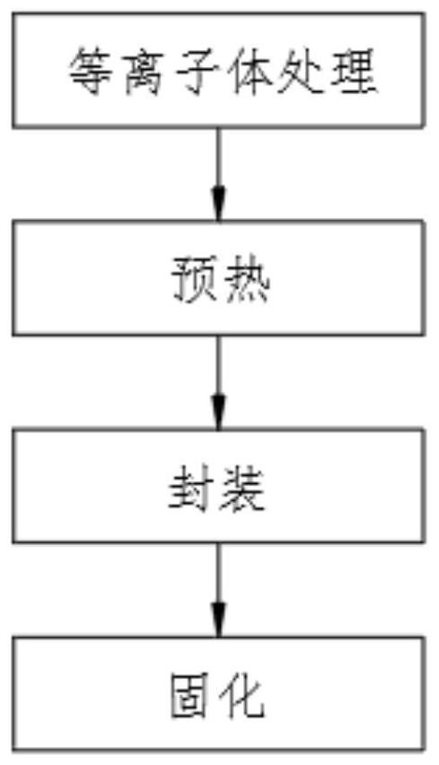
[0038] A fully automatic electronic component packaging process, comprising the steps of:

[0039] S1. Put the electronic components and packaging substrates into a vacuum chamber, and perform plasma treatment on the electronic components and packaging substrates in the presence of a gas containing an organosilicon compound;

[0040] S2. Preheating the electronic components after plasma treatment;

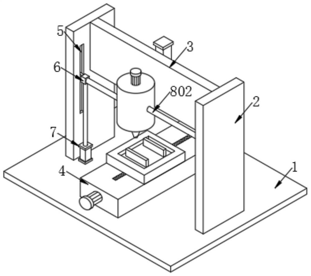
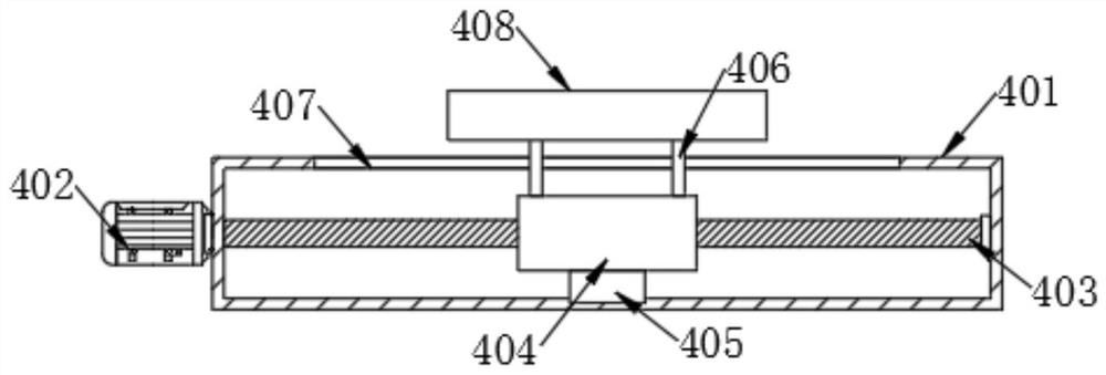
[0041] S3. Put the preheated electronic components on the suction cup 11 of the packaging equipment, use the dispensing mechanism 8 to apply the epoxy resin adhesive on the packaging substrate, and move the packaging substrate to the dispensing mechanism sequentially through the clamping mechanism 4 8 and under the suction cup 11, the electronic components are bonded to the packaging substrate through an epoxy resin adhesive;

[0042] S4. Put the packaging substrate bonded with the electronic components in a curing box for curing to complete the packaging process.

[0043] The pr...

Embodiment 2

[0048] A fully automatic electronic component packaging process, comprising the steps of:

[0049] S1. Put the electronic components and packaging substrates into a vacuum chamber, and perform plasma treatment on the electronic components and packaging substrates in the presence of a gas containing an organosilicon compound;

[0050] S2. Preheating the electronic components after plasma treatment;

[0051] S3. Put the preheated electronic components on the suction cup 11 of the packaging equipment, use the dispensing mechanism 8 to apply the epoxy resin adhesive on the packaging substrate, and move the packaging substrate to the dispensing mechanism sequentially through the clamping mechanism 4 8 and under the suction cup 11, the electronic components are bonded to the packaging substrate through an epoxy resin adhesive;

[0052] S4. Put the packaging substrate bonded with the electronic components in a curing box for curing to complete the packaging process.

[0053] The pr...

Embodiment 3

[0058] A fully automatic electronic component packaging process, comprising the steps of:

[0059] S1. Put the electronic components and packaging substrates into a vacuum chamber, and perform plasma treatment on the electronic components and packaging substrates in the presence of a gas containing an organosilicon compound;

[0060] S2. Preheating the electronic components after plasma treatment;

[0061] S3. Put the preheated electronic components on the suction cup 11 of the packaging equipment, use the dispensing mechanism 8 to apply the epoxy resin adhesive on the packaging substrate, and move the packaging substrate to the dispensing mechanism sequentially through the clamping mechanism 4 8 and under the suction cup 11, the electronic components are bonded to the packaging substrate through an epoxy resin adhesive;

[0062] S4. Put the packaging substrate bonded with the electronic components in a curing box for curing to complete the packaging process.

[0063] The pr...


PUM


Abstract

The invention relates to a full-automatic electronic component packaging process, which comprises the following steps of: S1, putting an electronic component and a packaging substrate into a vacuum chamber, and performing plasma treatment on the electronic component and the packaging substrate in the presence of gas containing an organic silicon compound; S2, preheating the electronic component subjected to plasma treatment; S3, putting the preheated electronic component on a suction cup of packaging equipment, coating the packaging substrate with an epoxy resin adhesive through a dispensing mechanism, sequentially moving the packaging substrate to the positions below the dispensing mechanism and the suction cup through a clamping mechanism, and bonding the electronic component to the packaging substrate through the epoxy resin adhesive; and S4, placing the packaging substrate bonded with the electronic component in a curing box for curing, thus completing the packaging process.

Description

technical field [0001] The invention relates to the technical field of electronic component packaging, in particular to a fully automatic electronic component packaging process. Background technique [0002] Packaging refers to connecting the circuit pins on the silicon chip to external joints with wires so as to connect with other devices; the packaging form refers to the shell used to install the semiconductor integrated circuit chip. It not only plays the role of installing, fixing, sealing, protecting the chip and enhancing the electrothermal performance, but also connects the contacts on the chip to the pins of the package shell with wires, and these pins pass through the wires on the printed circuit board. Connect with other devices to realize the connection between the internal chip and the external circuit. Because the chip must be isolated from the outside world to prevent impurities in the air from corroding the chip circuit and causing electrical performance degr...

Claims


Application Information

Patent Timeline
Patent Type & Authority Applications(China)
IPC IPC(8): H01L21/56H01L21/687H01L21/683H01L23/29
CPCH01L21/56H01L23/293H01L21/68764H01L21/68785H01L21/6838
Inventor 周海生蒋振荣
Owner 安徽富信半导体科技有限公司
Why Eureka
Try Eureka