Organic compound, electronic device comprising same, and electronic apparatus

A technology of organic compounds and chemical formulas, applied in the field of organic compounds and electronic devices and electronic devices containing them, to achieve the effects of high energy mobility, improved efficiency and life, and improved balance

Active Publication Date: 2021-10-26
SHAANXI LIGHTE OPTOELECTRONICS MATERIAL CO LTD
View PDF13 Cites 2 Cited by
  • Summary
  • Abstract
  • Description
  • Claims
  • Application Information

AI Technical Summary

Problems solved by technology

[0003] In the existing organic electroluminescent devices, the most important problems are life and efficiency. With the increase of the area of ​​the display, the driving voltage is also increased, and the luminous efficiency and current efficiency also need to be improved.

Method used


Image

  • Organic compound, electronic device comprising same, and electronic apparatus
  • Organic compound, electronic device comprising same, and electronic apparatus
  • Organic compound, electronic device comprising same, and electronic apparatus

Examples


Embodiment 1

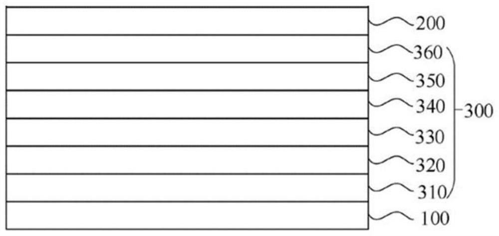
[0216] Embodiment 1: Preparation of red organic electroluminescent device

[0217] Anode preparation: the thickness of ITO / Ag / ITO is The ITO substrate is cut into a size of 40mm (length) × 40mm (width) × 0.7mm (thickness), and it is prepared into an experimental substrate with a cathode, an anode and an insulating layer pattern by using a photolithography process; ultraviolet ozone and O 2 :N 2 Plasma is used for surface treatment to increase the work function of the anode, and the surface of the ITO substrate is cleaned with an organic solvent to remove impurities and oil on the surface of the ITO substrate.

[0218] HAT-CN was vacuum evaporated on the experimental substrate (anode) to form a thickness of The hole injection layer (HIL), and then vacuum-evaporated NPB on the hole injection layer to form a thickness of the first hole transport layer.

[0219] On the first hole transport layer, compound HT-1 is vacuum evaporated to form a thickness of the second hole tr...

Embodiment 2-31

[0225] When forming the red light-emitting layer, an organic electroluminescent device was fabricated by the same method as in Example 1, except that the compound (Compound X) shown in Table 12 was substituted for Compound 1 in Example 1.


PUM


Abstract

The invention relates to an organic compound, an electronic device comprising the same, and an electronic apparatus comprising the electronic device. The structural formula of the organic compound is shown as a chemical formula 1, and the organic compound is applied to the electronic device and can remarkably improve the performance of the electronic device.

Description

technical field [0001] The application belongs to the technical field of organic materials, and in particular relates to an organic compound and an electronic device and electronic device containing the same. Background technique [0002] An organic electroluminescence device, such as an organic light emitting diode (OLED), generally includes a cathode and an anode oppositely arranged, and a functional layer arranged between the cathode and the anode. The functional layer is composed of multiple organic or inorganic film layers, and generally includes an organic light-emitting layer, a hole transport layer, an electron transport layer, and the like. When a voltage is applied to the cathode and anode, the two electrodes generate an electric field. Under the action of the electric field, the electrons on the cathode side move to the electroluminescent layer, and the holes on the anode side also move to the light-emitting layer, and the electrons and holes combine in the electr...

Claims


Application Information

Patent Timeline
Patent Type & Authority Applications(China)
IPC IPC(8): C07D405/04C07D405/14C07D409/14C07D405/10C09K11/06H01L51/54
CPCC07D405/04C07D405/14C07D409/14C07D405/10C09K11/06C09K2211/1059C09K2211/1092C09K2211/1088C09K2211/1029H10K85/654H10K85/6576H10K85/6574Y02E10/549
Inventor 徐先彬金荣国张鹤鸣
Owner SHAANXI LIGHTE OPTOELECTRONICS MATERIAL CO LTD
Why Eureka
Try Eureka