Equipment suitable for resistivity measurement pretreatment of silicon epitaxial wafer
A silicon epitaxial wafer, resistivity technology, used in semiconductor/solid-state device testing/measurement, circuits, discharge tubes, etc. The effect of reducing the difficulty and cost of processing and reducing production costs
- Summary
- Abstract
- Description
- Claims
- Application Information
AI Technical Summary
Problems solved by technology
Method used
Image
Examples
Embodiment
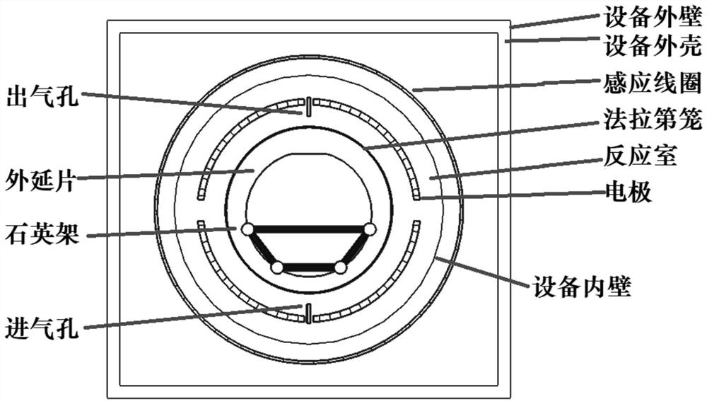
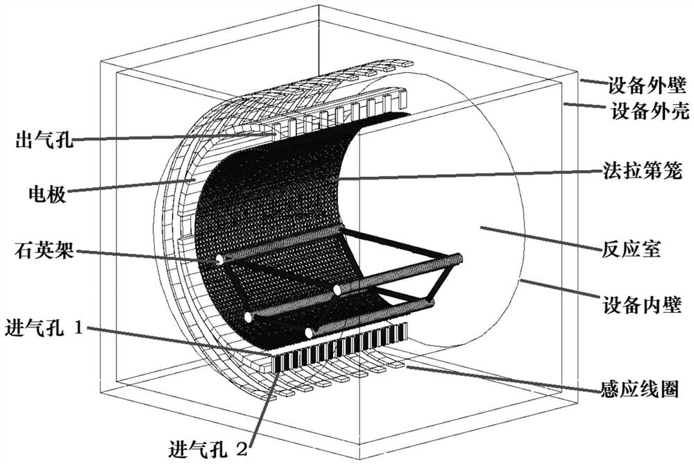
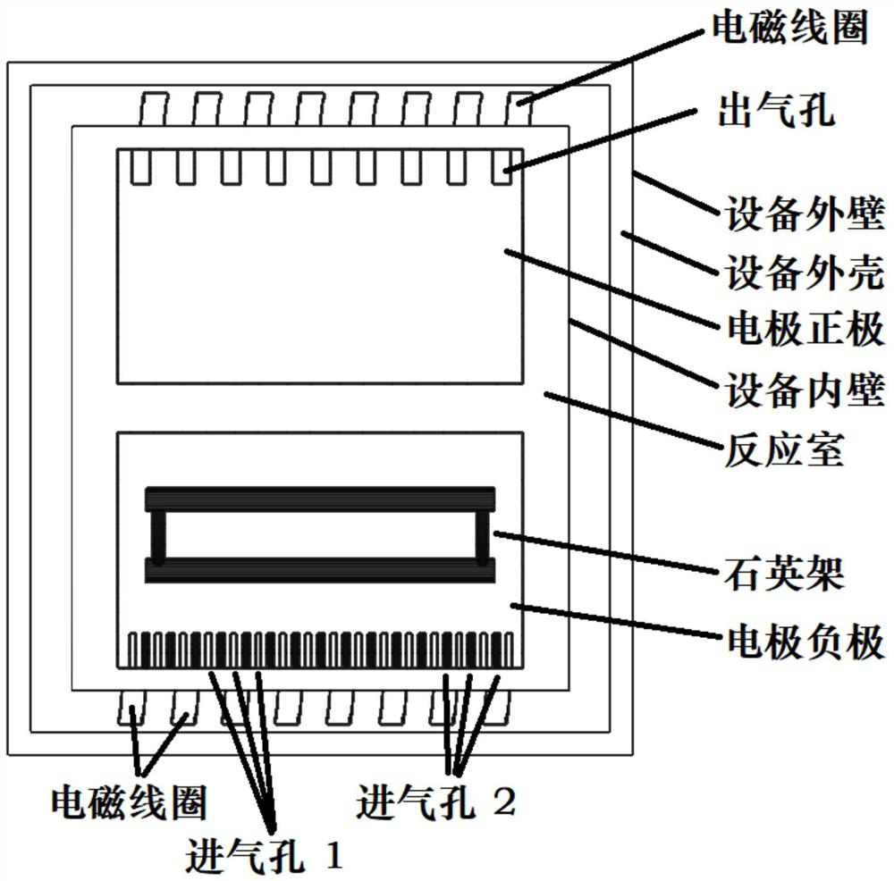
[0051] In a specific embodiment, such as figure 1 , figure 2 , image 3 , Figure 4 , Figure 5 with Image 6As shown, a device suitable for pre-treatment of silicon epitaxial wafer resistivity measurement, including equipment inner wall, equipment outer wall, equipment shell, reaction chamber, quartz frame, electrode, air inlet, air outlet, induction coil; the reaction chamber Located in the inner wall of the device, the induction coil is located outside the inner wall of the device, the electrodes are located inside the reaction chamber and placed oppositely, the quartz frame is placed inside the electrodes, and the air inlet is located in the On the negative electrode side of the electrode, the gas outlet is located on the positive electrode side of the electrode, and the gas inlet and the outlet gas are not in contact with the electrode.
[0052] In this embodiment, the size of the outer wall of the device is 30×40×40 centimeters in length, width and height.
[0053...
PUM
| Property | Measurement | Unit |
|---|---|---|
| Diameter | aaaaa | aaaaa |
| Diameter | aaaaa | aaaaa |
Abstract
Description
Claims
Application Information
 - R&D Engineer
- R&D Manager
- IP Professional
- Industry Leading Data Capabilities
- Powerful AI technology
- Patent DNA Extraction
Browse by: Latest US Patents, China's latest patents, Technical Efficacy Thesaurus, Application Domain, Technology Topic, Popular Technical Reports.
© 2024 PatSnap. All rights reserved.Legal|Privacy policy|Modern Slavery Act Transparency Statement|Sitemap|About US| Contact US: help@patsnap.com


