Broadband Transition Structure Between Grounded Coplanar Waveguide and Stripline with Curved Grounding Electrode

A grounded coplanar waveguide and grounded electrode technology, used in waveguide-type devices, circuits, connecting devices, etc., can solve problems such as through-hole size requirements, limited operating bandwidth, electromagnetic leakage, etc., to reduce reflection coefficient and insertion loss, Avoid opening holes on the ground plane and reduce the effect of electromagnetic leakage

Active Publication Date: 2022-03-15
SHANGHAI JIAOTONG UNIV
View PDF6 Cites 0 Cited by
  • Summary
  • Abstract
  • Description
  • Claims
  • Application Information

AI Technical Summary

Problems solved by technology

In order to realize the transition structure from the grounded coplanar waveguide to the stripline, the conduction bands of the grounded coplanar waveguide and the stripline are connected by a through-silicon via (TSV). Generally, electrodes larger than the cross-section of the TSV are required. The dimensional changes of the conduction band and electrodes and the discontinuity of the TSV will introduce significant parasitic effects at high frequencies, limiting the operating bandwidth of the grounded coplanar waveguide to stripline transition structure.
To solve this problem, at present, metallized via holes with a smaller radius matching the conduction band are mainly used, and at the same time, holes are opened at the corresponding positions of the metal ground plane to offset the parasitic capacitance effect introduced by the pad or through step drilling. , but this type of technology has requirements on the size of the through hole, and at the same time, the opening of the ground plane will cause electromagnetic leakage, which will have a negative impact on the working characteristics and compatibility of the device, interconnection and system, or it is necessary to increase the number of substrate stacking layers and in the substrate Air grooves are formed in the bottom, which significantly increases the process complexity

Method used


Image

  • Broadband Transition Structure Between Grounded Coplanar Waveguide and Stripline with Curved Grounding Electrode
  • Broadband Transition Structure Between Grounded Coplanar Waveguide and Stripline with Curved Grounding Electrode
  • Broadband Transition Structure Between Grounded Coplanar Waveguide and Stripline with Curved Grounding Electrode

Examples


Embodiment Construction

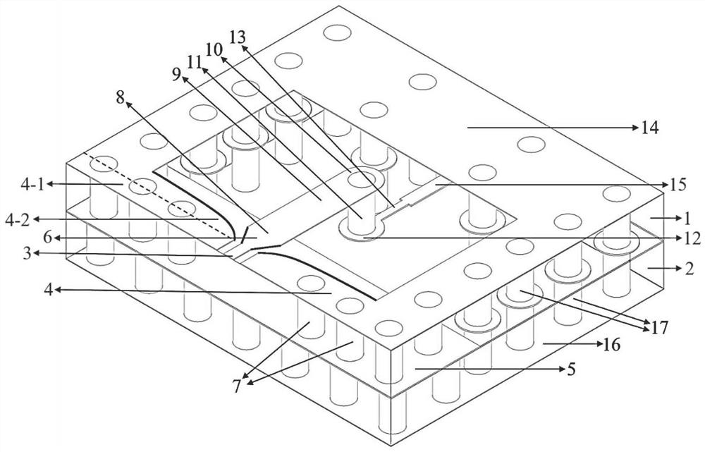
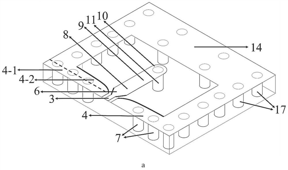
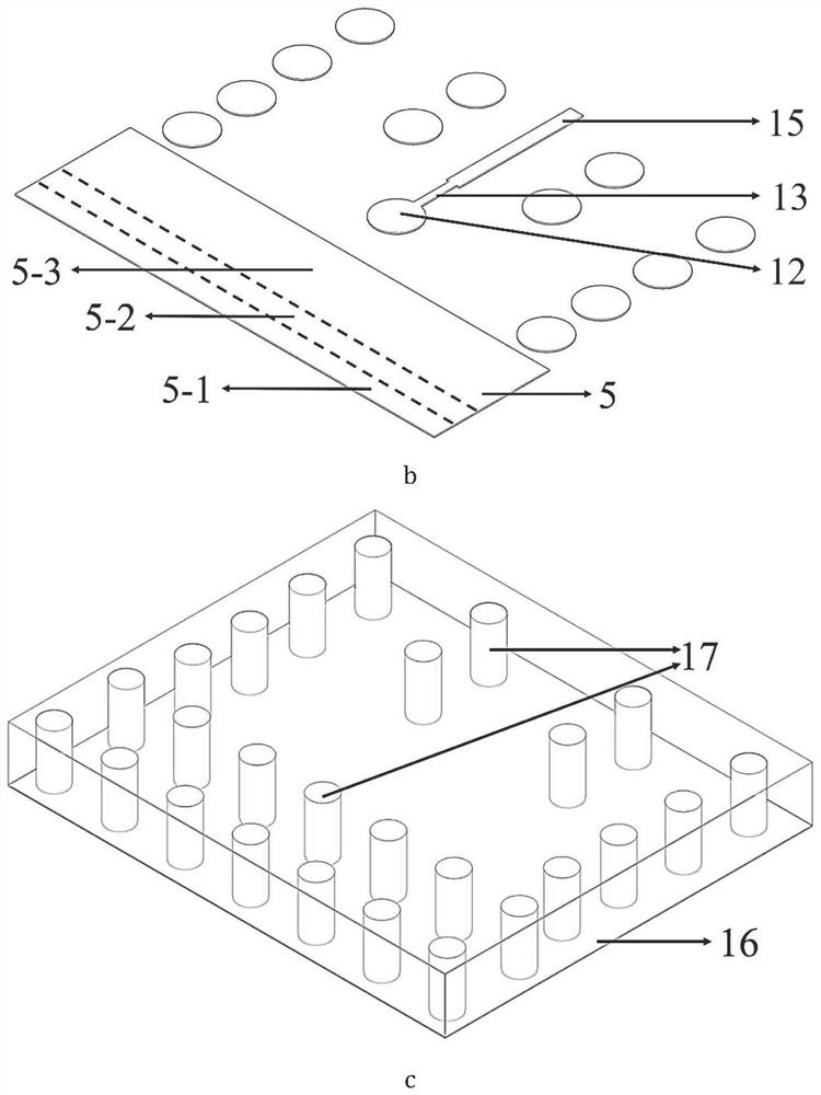
[0027] Such as figure 1 , figure 2 As shown, it is a broadband transition structure between a grounded coplanar waveguide and a stripline with a curved ground electrode in this embodiment. , the gradient grounded coplanar waveguide unit and the stripline unit, and the microstrip line unit, the first stripline 9, the through-silicon via (TSV) unit and the second Strip line 13.

[0028] The thicknesses of the upper silicon wafer 1 and the lower silicon wafer 2 are both h, and the relative dielectric constant is ε r .

[0029] The uniformly grounded coplanar waveguide unit includes: a uniformly grounded coplanar waveguide strip 3 arranged on the upper surface of the upper silicon chip 1, rectangular ground electrodes 4-1 symmetrically arranged on both sides of the grounded coplanar waveguide strip 3, and A uniformly grounded coplanar waveguide ground 5-1 arranged between the upper silicon wafer 1 and the lower silicon wafer 2.

[0030] The width of the uniformly grounded co...


PUM


Abstract

A broadband transition structure between a grounded coplanar waveguide and a stripline with a curved ground electrode, comprising: stacked two-layer silicon wafers, uniformly grounded coplanar waveguide units, gradient grounded coplanar waveguide units, and striplines arranged in sequence The unit and the microstrip line unit, the first strip line, the through-silicon via unit and the second strip line connected sequentially inside the gradient ground coplanar waveguide unit and the strip line unit. The invention adopts the grounding electrode whose edge changes in a curve with the width of the equivalent trapezoidal conduction strip, so as to ensure that the characteristic impedance of the gradually changing grounded coplanar waveguide is always the standard impedance; the width and length of the stripline are optimized, so that the equivalent inductance of the stripline and the TSV is equal to the The gap equivalent capacitances are balanced with each other to achieve broadband impedance matching. The device does not need to open a hole on the ground plane, does not increase the complexity of the process, can achieve a large working bandwidth, and meets the requirements of the three-dimensional interconnection network in the silicon-based three-dimensional integrated circuit for broadband and low-loss transmission of radio frequency millimeter wave signals.

Description

technical field [0001] The invention relates to a technology in the field of three-dimensional integrated circuits, in particular to a broadband transition structure of a grounded coplanar waveguide with a curved ground electrode and a stripline. Background technique [0002] In silicon-based three-dimensional integrated circuits, grounded coplanar waveguides, striplines and their transfer transition structures are usually cascaded in the transmission network, so the operating bandwidth and insertion loss of the transition structure have a great influence on the performance of the entire interconnection network. Large impact, it is necessary to carry out broadband and low loss design for the transition structure from grounded coplanar waveguide to stripline. In order to realize the transition structure from the grounded coplanar waveguide to the stripline, the conduction bands of the grounded coplanar waveguide and the stripline are connected by a through-silicon via (TSV). ...

Claims


Application Information

Patent Timeline
Patent Type & Authority Patents(China)
IPC IPC(8): H01P5/107
CPCH01P5/107
Inventor 吴林晟李晨晨毛军发侯芳朱健
Owner SHANGHAI JIAOTONG UNIV
Why Eureka
Try Eureka