A kind of preparation method of double-sided MWT-hit cell assembly
A battery module and double-sided technology, applied in electrical components, circuits, photovoltaic power generation, etc., can solve the problems of poor cost performance, high unit price of low-temperature silver paste consumption, and difficulty in realizing low-cost double-sided, so as to reduce consumption, The effect of reducing the cost of electricity and increasing the comprehensive power generation
- Summary
- Abstract
- Description
- Claims
- Application Information
AI Technical Summary
Problems solved by technology
Method used
Image
Examples
Embodiment 1
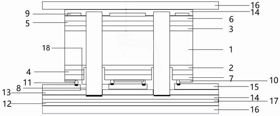
[0059] This embodiment is a double-sided MWT-Hit battery assembly, which includes a frontal ultra-white high-transverse glass, a front package polymer, a front electrode, a front electrode, a front TCO layer, a front N +-doped amorphous silicon layer, a front Essentially amorphous silicon passage, N-type single crystal silicon substrate, back surface intrinsic amorphous silicon passive layer, back surface P-type doped amorphous silicon emission layer, back surface TCO layer, back electrode ring, second back electrical conductive The foil, the second back side high permeable polymer, the first back surface conductive foil, the back coloring film, the first back surface high pass insulating polymer, the back surface is super white and high transmissions. The back of the battery is consistent with the front pattern height, and the back and rigging pattern is only designed at the electrode point, forming a back electrode ring surrounding the front electrode electrode point. The back e...
Embodiment 2
[0070] In another aspect, the present invention provides a process for process preparation of a double-sided MWT-Hit battery assembly, the process preparation method comprising the following process steps:
[0071] S01 performs laser punching of N-silicon wafers;
[0072] S02 silicon wafer cleaning polishing: Filip and cleaning of the n-type single crystal silicon substrate, removing a mechanical damage layer and contaminant on the surface of the silicon substrate, forming a pyramid suction surface;
[0073] S03 double-sided deposition intrinsic amorphous silicon layer;
[0074] N-type amorphous silicon deposition is performed on the front of S04;
[0075] S05 on the back of the S05 for deposition of P-type amorphous silicon;
[0076] TCO deposition is performed on the front of S06;
[0077] S07 on the back of the S07 for TCO deposition;
[0078] The back surface of the S08 is periphered by the position of the bore to perform local etching of the back surface TCO and P-type amorph...
Embodiment 3
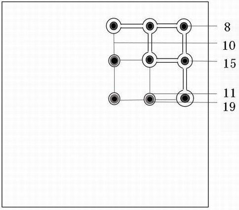
[0086] The present application also provides an integrated composite local domain conductive core panel to ensure that the embodiments of the present invention are more clear and described below. by figure 2 Taking an example, figure 2 Rear view of the MWT-HIT battery. The integrated complexed domain conductive core panels in the present invention are mainly in contact with the back surface of the MWT-Hit battery and laminated. Need to be in front of the contact lamination package figure 2 The conductive glue is printed on the back negative electrode point and the back electrode ring shown in the back electrode ring. The cover is then performed in the following order.
[0087] 1. The second back surface conductive foil is covered, the circular ring region in the second back surface conductive foil completely covers the back electrode ring, and effectively connects the conductive through the conductive glue on the back electrode ring. The requirements for the conductive glue printi...
PUM
 Abstract
Description
Claims
Application Information


