Memory and manufacturing method thereof
A memory and storage layer technology, which is applied in semiconductor/solid-state device manufacturing, transistors, electrical components, etc., to save occupied area and complexity, facilitate miniaturization and high integration, and save surface area
- Summary
- Abstract
- Description
- Claims
- Application Information
AI Technical Summary
Problems solved by technology
Method used
Image

Examples
Embodiment Construction
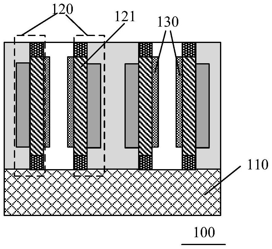
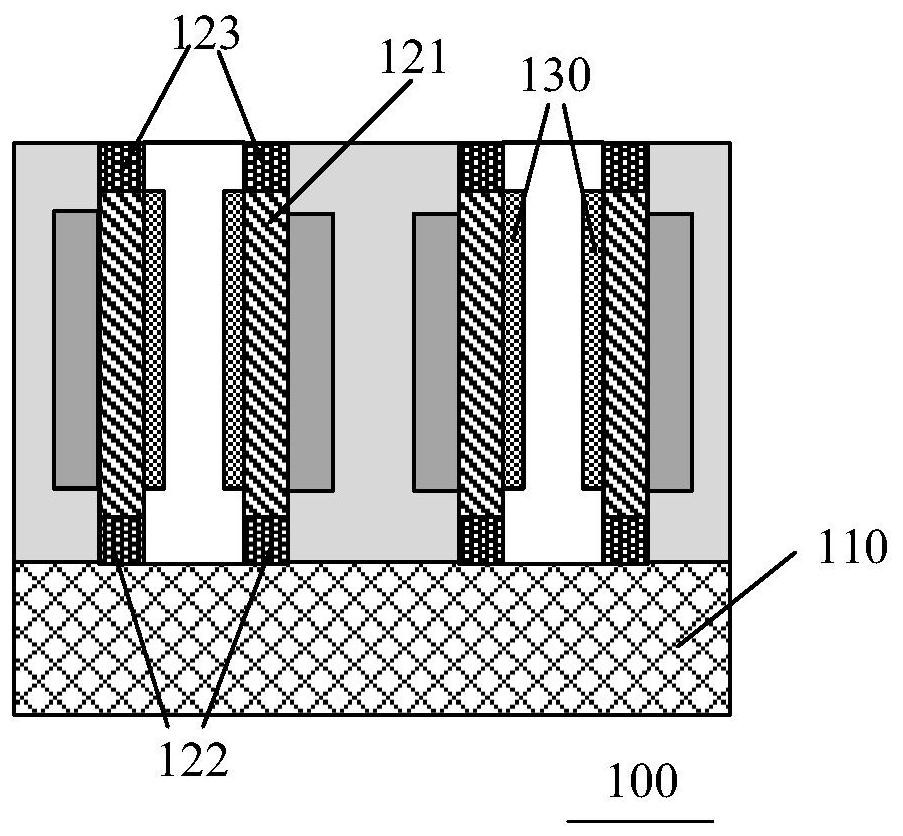
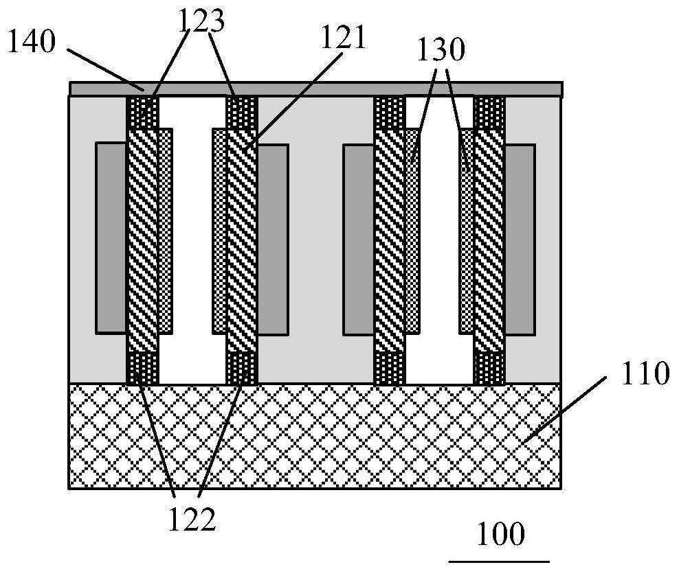
[0081] The technical solutions of the present application can be applied to the design and manufacture of semiconductor memories, for example, commonly used semiconductor memories such as DRAM. A common DRAM uses a capacitor to store charges, and the value of a binary bit (bit) is represented by the amount of charge stored, that is, a storage unit can be used to represent a logic state of a bit. Due to phenomena such as leakage current in the transistor, the stored charge is prone to loss, thereby affecting the stability of data storage. Therefore, DRAM needs to be periodically charged and discharged, and the stored data is refreshed to realize dynamic storage.
[0082] Considering that the capacitor structure requires two capacitor plates and a dielectric layer, it needs to occupy a large space size, which makes it difficult to reduce the size of a single storage unit, and the overall size of the memory is also limited by this bottleneck. Therefore, the embodiment of the pre...
PUM
 Abstract
Description
Claims
Application Information
 - Generate Ideas
- Intellectual Property
- Life Sciences
- Materials
- Tech Scout
- Unparalleled Data Quality
- Higher Quality Content
- 60% Fewer Hallucinations
Browse by: Latest US Patents, China's latest patents, Technical Efficacy Thesaurus, Application Domain, Technology Topic, Popular Technical Reports.
© 2025 PatSnap. All rights reserved.Legal|Privacy policy|Modern Slavery Act Transparency Statement|Sitemap|About US| Contact US: help@patsnap.com