High-end PMOS power tube driving circuit

A MOS tube and drive circuit technology, applied in the field of high-end PMOS power tube drive circuits, can solve the problems of difficult integration, power tube breakdown, and complex gate-source voltage clamping circuits of power tubes, so as to improve circuit integration and reduce conduction. The effect of reducing the transmission loss, reducing the cost of use and the area of ​​use

Active Publication Date: 2021-11-05
XIDIAN UNIV
View PDF3 Cites 2 Cited by
  • Summary
  • Abstract
  • Description
  • Claims
  • Application Information

AI Technical Summary

Problems solved by technology

However, it has the following disadvantages: it is necessary to use an external chip capacitor to charge and discharge the grid capacitance of the power tube, the circuit area is large and it is not easy to integrate; the gate-source voltage clamping circuit of the power tube is complex, which is easy to cause reliability such as breakdown of the power tube question

Method used


Image

  • High-end PMOS power tube driving circuit
  • High-end PMOS power tube driving circuit
  • High-end PMOS power tube driving circuit

Examples


Embodiment 1

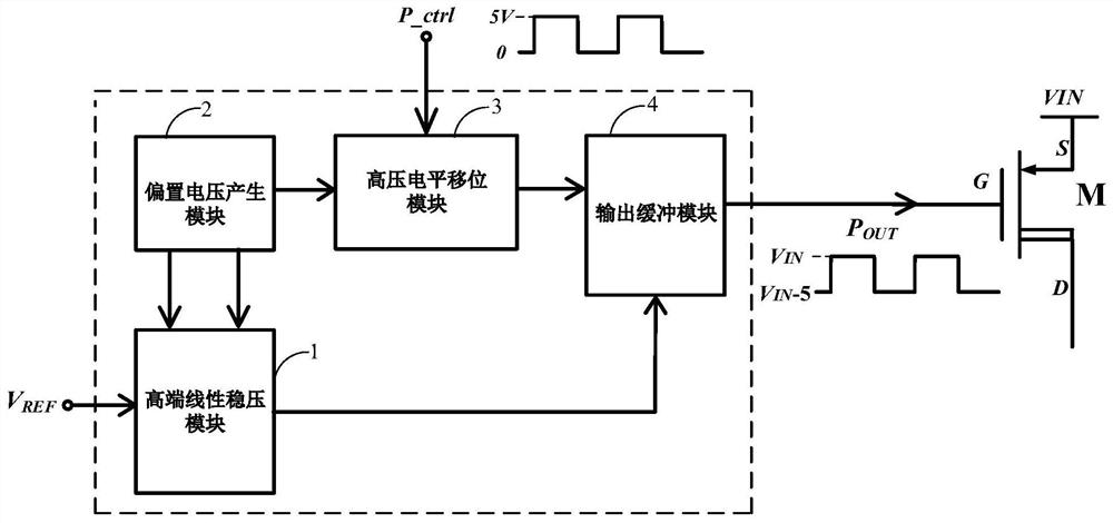
[0079] See figure 1 , figure 1 Is a block diagram of a high-end PMOS power transistor drive circuit according to an embodiment of the present invention, as shown in FIG high PMOS power transistor drive circuit of this embodiment includes: a high linear voltage regulator, the bias voltage generating module 2 , high voltage level shifting module 3 and the output buffer module 4. Wherein the output of the linear regulator-end module 1 is connected to the input of output buffer module 4, the bias voltage generator 2 is connected to the output of the module-end linear regulator module input terminal 1 and the high voltage level shift the input module 3, respectively, input terminal, a high voltage level shift module 3 is connected to the output terminal of output buffer module 4, the output terminal of the output buffer module of P 4 OUT End connected to the gate of the PMOS power transistor M.

[0080] In particular, high linear regulator module 1 according to the reference voltage in...


PUM


Abstract

The invention relates to a high-end PMOS power tube driving circuit, and the circuit comprises a high-end linear voltage stabilization module, a bias voltage generation module, a high-voltage level shift module and an output buffer module, wherein the high-end linear voltage stabilization module is used for generating a control level according to an input reference voltage signal VREF; the bias voltage generation module is used for generating a bias level and providing a bias voltage for the high-end linear voltage stabilization module and the high-voltage level shift module; and the high-voltage level shifting module is used for performing level shifting on the input first square wave control signal Pctrl and converting the input first square wave control signal Pctrl into a second square wave control signal Pctrl-hs to be output. And the output buffer module is used for charging or discharging the grid electrode of the high-end PMOS power tube according to the second square wave control signal P_ctrl-hs so as to control the high-end PMOS power tube to be turned on or turned off. According to the drive circuit, the gate-source voltage of the high-end PMOS power tube can be effectively controlled within the safety voltage, the high-end PMOS power tube is conducted to the maximum extent, and the conduction loss is reduced.

Description

Technical field [0001] The present invention belongs to the field of integrated circuit technology, particularly, to a high-power transistor PMOS driver circuit. Background technique [0002] With the rapid development of IC industry in my country in recent years, with high integration, high reliability, low cost and other advantages of smart power integrated circuit (SPIC) is widely used. In SPIC, the bridge driver circuit due to its topology and control method is widely used and simple. In selecting high-power transistor bridge circuit, the use of NMOS power control, the need to generate a higher voltage than the input level to turn on the power NMOS normal tube, it is often necessary bootstrap capacitor, a power diode, an outer sheet member. This not only increases the cost and use of space, but also bring additional reliability problems due to electromagnetic interference and so on. [0003] Appropriate way to solve these problems is to use a tube as a high power PMOS switch,...

Claims


Application Information

Patent Timeline
Patent Type & Authority Applications(China)
IPC IPC(8): H02M1/08H03K17/687
CPCH02M1/08H03K17/687
Inventor 张艺蒙丁允张玉明汤晓燕宋庆文
Owner XIDIAN UNIV
Why Eureka
Try Eureka