FCM packaging chip machine manufacturing method, packaging chip machine and camera module product

A production method and a technology of encapsulating chips, which are applied in image communication, radiation control devices, televisions, etc., can solve problems such as difficult production process control, high product costs, and decreased product reliability, so as to reduce equipment investment costs and The effect of labor cost, high market competitive advantage, and product yield improvement

Inactive Publication Date: 2021-11-09
SHENZHEN E WELLY ELECTRONICS
View PDF0 Cites 5 Cited by
  • Summary
  • Abstract
  • Description
  • Claims
  • Application Information

AI Technical Summary

Problems solved by technology

[0010] The flatness of the FPC material SMT cannot be controlled after the furnace, which eventually leads to poor module tilt and low yield
[0011] The use of FPC circuit boards requires the use of a large number of high-density gold wires as electrical connect

Method used


Image

  • FCM packaging chip machine manufacturing method, packaging chip machine and camera module product
  • FCM packaging chip machine manufacturing method, packaging chip machine and camera module product
  • FCM packaging chip machine manufacturing method, packaging chip machine and camera module product

Examples


specific Embodiment approach 1

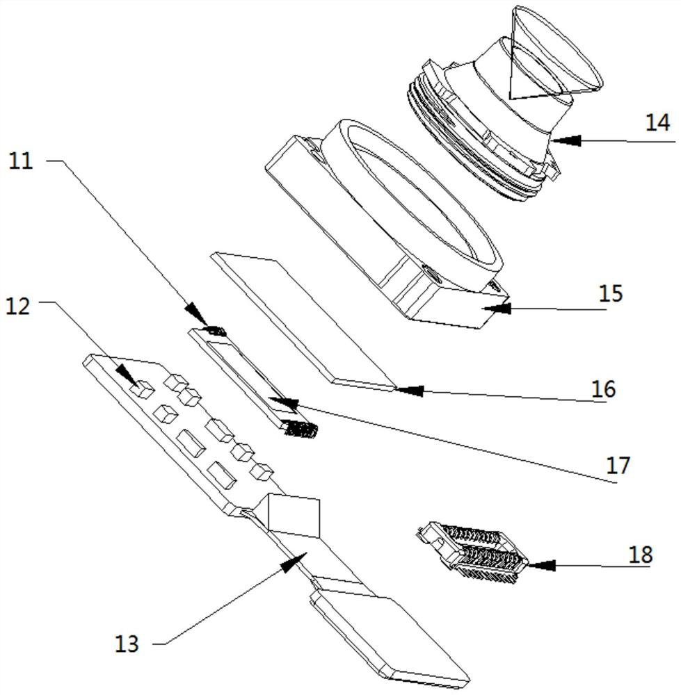
[0073] FCM production process: see Figure 10 ;

[0074] Step 1: Die the copper foil with a knife die and bend it into a circuit;

[0075] Step 2: use spot plating process (spot plating process: one of the electroplating processes, which can electroplate the designated position) to plate the circuit with nickel and gold;

[0076] Step 3: Injection molding through the inster molding process (the inster molding process is the insert molding process: a molding method in which the metal is embedded in a pre-fabricated mold cavity, and then the molten plastic material is injected); in this step, the step In 2, the nickel and gold-plated circuits are embedded in the prefabricated mold cavity, and then the molten plastic material is injected for injection molding;

[0077] Step 4: After molding, inject solder paste, attach capacitors, resistors and other electronic components, and fix them by reflow soldering;

[0078] Step 5: Then turn over and paint the adhesive filter, bake and...

specific Embodiment approach 2

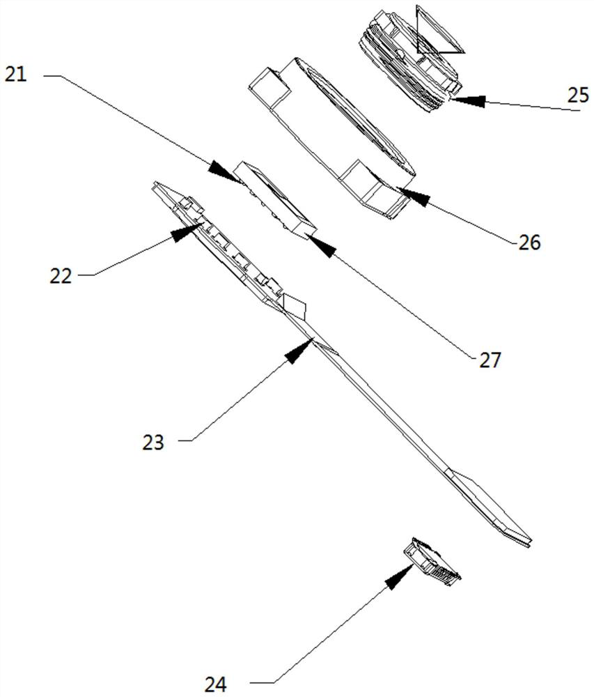
[0082] Such as Figure 7 , another production process of FCM: see Figure 11 ;

[0083] Step 1: Die the copper foil with a knife die and bend it into a circuit;

[0084] Step 2: use spot plating process (spot plating process: one of the electroplating processes, which can electroplate the designated position) to plate the circuit with nickel and gold;

[0085] Step 3: Injection molding by inster molding process (inster molding process: a molding method in which metal is embedded in a prefabricated mold cavity, and then molten plastic material is injected); in this step, nickel is plated in step 2 Embed the circuit with gold into the prefabricated mold cavity, and then inject the molten plastic material into injection molding;

[0086] Step 4: Inject solder paste after molding, and paste electronic components such as capacitors and resistors;

[0087] Step 5: Simultaneously weld the chip with a laser solder ball welding machine to solder solder balls;

[0088] Step 6: Conn...


PUM


Abstract

The invention provides an FCM packaging chip machine manufacturing method, a packaging chip machine and a camera. A small-sized camera which is provided with an FCM and does not need a circuit board comprises a lens, a base and the FCM, the FCM mainly utilizes a camera module packaging sheet (Flip Chip Module for short) which is manufactured by combining an FPC-free circuit board lead bracket and an advanced semiconductor packaging technology (Flip Chip), and the FCM is a packaging sheet module integrating an optical filter, an image chip, a driving/storage chip, an electronic component and a connector into a whole). According to the scheme, a circuit board is not needed to serve as a connection bridge any more, meanwhile, most precise assembly procedures are saved, and equipment and manpower cost investment is reduced. Moreover, the accumulated tolerance of the simplified assembly process is also reduced, the offset and inclination can be better controlled, and the product yield is improved.

Description

technical field [0001] The invention relates to the field of electronic product accessories, in particular to a small camera and a method for manufacturing the camera packaging sheet. Background technique [0002] Such as figure 1 and figure 2 as shown, figure 1 : The COB camera in the prior art, the names of the components in the figure are as follows: gold wire 11, electronic components 12 such as capacitors and resistors, circuit board 13, lens 14, base 15, optical filter 16, chip 17, connector 18; figure 2 : the CSP camera in the prior art, the part names in the figure are as follows: electronic components 22, circuit board 23, connector 24, lens 25, base 26, chip 27 such as tin ball 21, electric capacity, resistance. [0003] The main features of the conventional COB / CSP small camera module are: use the nickel-palladium-gold circuit board (FPCB) as the substrate, first use the SMT process to mount the components such as resistors, capacitors, connectors, drive / stor...

Claims


Application Information

Patent Timeline
IPC IPC(8): H01L27/146H04N5/225
CPCH01L27/1469H01L27/14634H04N23/50H04N23/55
Inventor 李东
Owner SHENZHEN E WELLY ELECTRONICS
Why Eureka
Try Eureka