Semiconductor epitaxial structure and preparation method thereof, and LED chip
An LED chip and epitaxial structure technology, applied in semiconductor devices, electrical components, circuits, etc., can solve the problems of unfavorable red LED antistatic devices, restricting the utilization rate of light-emitting area, and speeding up the aging speed of chips, etc., to facilitate current expansion. , the effect of enhancing the current expansion capability and increasing the current expansion capability
- Summary
- Abstract
- Description
- Claims
- Application Information
AI Technical Summary
Problems solved by technology
Method used
Image
Examples
Embodiment 1
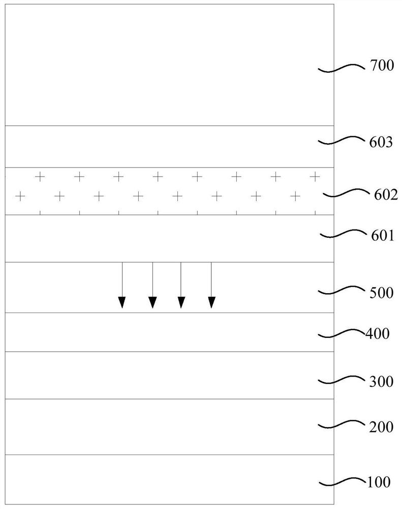
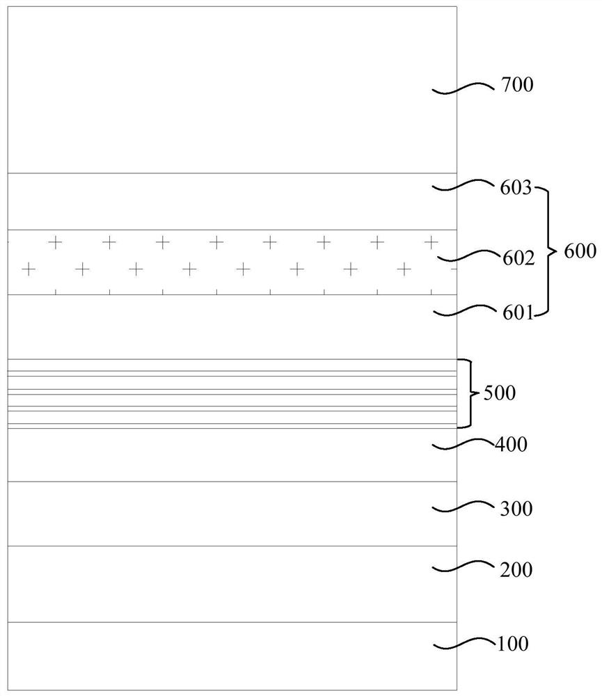
[0071] This embodiment provides a semiconductor epitaxial structure, referring to figure 2 and image 3 , the epitaxial structure includes: a growth substrate 100, having a first surface and a second surface oppositely disposed; a first current spreading layer 500, disposed above the first surface of the growth substrate 100; an epitaxial layer 600, disposed on the second The surface of a current spreading layer 500 , and the epitaxial layer 600 sequentially includes a first semiconductor layer 601 , an active layer 602 and a second semiconductor layer 603 ; the second current spreading layer 700 is disposed above the second semiconductor 603 . Wherein, the first current spreading layer 500 includes first doped layers 501 and second doped layers 502 arranged alternately, and the doping concentration of the first doped layers 501 is greater than that of the second doped layers 502 . Since the doping concentration of the first doped layer 501 is relatively large, it is conduci...
Embodiment 2
[0078] This embodiment provides a kind of LED chip, refer to image 3 , Figure 4 and Figure 5 , the LED chip includes: a substrate 900, having a first surface and a second surface oppositely disposed; a second current spreading layer 700, located above the substrate 900; an epitaxial layer 600, located above the second current spreading layer 700, the epitaxial layer 600 sequentially includes a second semiconductor layer 603, an active layer 602, and a first semiconductor layer 601 on the surface of the second current spreading layer 700; the first current spreading layer 500 is located above the first semiconductor layer 601, and the first current The extension layer 500 includes first doped layers 501 and second doped layers 502 arranged alternately, and the doping concentration of the first doped layers 501 is greater than that of the second doped layers 502 .
[0079] Specifically, refer to Figure 4 or Figure 5 , the substrate 900 includes but not limited to Mo sub...
Embodiment 3
[0088] This embodiment provides a method for preparing a semiconductor epitaxial structure, referring to Image 6 , including the following steps:
[0089] S101: Provide a growth substrate, the growth substrate has a first surface and a second surface oppositely arranged;
[0090] refer to figure 2 1. A growth substrate 100 is provided. The material of the growth substrate 100 includes but not limited to GaAs. In this embodiment, the GaAs growth substrate 100 is taken as an example.
[0091] refer to figure 2 , the buffer layer 200, the etch stop layer 300, and the ohmic contact layer 400 are sequentially formed on the first surface of the growth substrate 100, specifically, the chemical vapor deposition method may be used to sequentially deposit them. Wherein, the etch stop layer 300 is an N-type etch stop layer 300 made of N-GaInP; the material of the ohmic contact layer 400 is N-GaAs.
[0092] S102: Forming a first current spreading layer including alternately arrange...
PUM
| Property | Measurement | Unit |
|---|---|---|
| thickness | aaaaa | aaaaa |
| thickness | aaaaa | aaaaa |
| area | aaaaa | aaaaa |
Abstract
Description
Claims
Application Information


